– Imaging of functional group distribution on carbon nanotube bundle structures –
Researchers: NAKAJIMA Hideaki, AIST Postdoctoral Researcher, MORIMOTO Takahiro, Senior Researcher, KOBASHI Kazufumi, Senior Researcher, and OKAZAKI Toshiya, Leader and Research Center Deputy Director, CNT Characterization Team, CNT-Application Research Center
- Novel elemental analysis technique with high spatial resolution of < 10 nm in a scanning electron microscope (SEM) has been developed.
- The technique enables the evaluation of spatial uniformity relating to functional groups on fine bundles of carbon nanotubes.
- The technique is of importance for advancing the development of various nanomaterials as a novel method for analyzing their surface states.
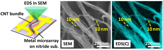
Highly spatially resolved energy dispersive X-ray spectrometry (EDS) measurement in SEM
Carbon nanotubes (CNTs) exhibit excellent electrical, mechanical, and thermal properties and have potential for various nanotechnology applications such as stretchable electronics devices and conductive composite materials. However, CNTs easily form bundles and aggregated structures due to strong van der Waals force. In this point, functionalization of CNTs is a key technique for improving the dispersibility in solution and polymer matrices. Although several imaging techniques for transmission electron microscope (TEM) can characterize the spatial distribution of elements chemically bound to an isolated CNT surface, they are unsuitable for examinations on a practical scale because of their limited scanning area. Therefore, to evaluate the overall properties of CNT dispersions containing bundles of various sizes, a scalable examination with both a large scanning area and sufficient spatial resolution is required.
In this work, a novel elemental imaging technique with EDS in SEM has been developed realizing sufficient spatial resolution of 10 nm, in collaboration with the New Energy and Industrial Technology Development Organization (NEDO). This work was conducted as part of NEDO's "Ultra-high-speed Development of Ultra-advanced Materials Foundation Project."
EDS measurement in SEM is widely used as a quantitative evaluation method of the spatial distribution relating to surface state of various materials. However, due to the low analytical sensitivity of EDS to light elements, the spatial resolution is limited to around 1 µm which hinders acquisition of spatial information from individual CNT bundles. In the developed technique, highly stabilized X-ray signal detection is realized by using a modified sample support substrate, enabling to image CNT bundle structure with sufficient spatial resolution of less than 10 nm.
The technique enables quantitative evaluation of the spatial distribution of degree of functionalization of a CNT bundle surface. Furthermore, it can be widely applicable to not only CNTs but also various nanomaterials with a practical measurement area.