– Development of a double-sided interferometer for thickness measurement traceable to the national standards for length –
Researchers: HIRAI Akiko, Leader, Nanoscale Standards Group, Research Institute for Engineering Measurement, and BITOU Youichi, Leader, Length Standards Group, Research Institute for Engineering Measurement
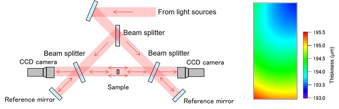
The researchers have developed a double-sided interferometer for thickness measurement that can measure the thickness of a silicon wafer without being affected by the refractive index inside the wafer. The thickness distribution of a 200 μm thick silicon wafer was measured with high precision.
 |
|
Left: The developed double-sided interferometer for thickness measurement. Right: Thickness measurement results of 30 × 10 mm wafer |
The spectral interference method using interference between the light beams reflected from a front surface and a back surface of a sample is widely used for non-contact measurement of thickness. With this method, light is transmitted through the sample, so measurement results are affected by the refractive index. Because the refractive index varies from one lot to the next and is dependent on the additive concentration, reliability of results from this method cannot be guaranteed. There is need for an interferometer for thickness measurement that is free from the effect of refractive index of the sample.
The developed method uses only front surface reflected light to measure the surface shape on both sides of the sample with two optical interferometers and determine the thickness. Because the method does not use transmitted light, it is not affected by the refractive index of the sample. Using frequency-stabilized lasers as the light sources, it can measure thickness with high precision. The researchers measured the thickness of block gauges with thicknesses of 1 to 30 mm using the developed method and confirmed that it had a precision of ±10 nm. The researchers measured the thickness distribution of a silicon wafer with high precision, proving that the wafer can be used as a standard sample for device calibration.
In the future, the researchers will examine the applicability of the developed method to thinner silicon wafers for lamination. They will also expand the range of thicknesses that can be measured.