– Significantly improved production efficiency of next-generation electronic materials utilizing nano-carbons –
AIST has developed a technology to easily manufacture high-purity thin films simply by irradiating a dispersion of nano-carbon materials with light. Patterning is possible on substrates with curved surfaces and uneven surfaces of various materials.
 |
|
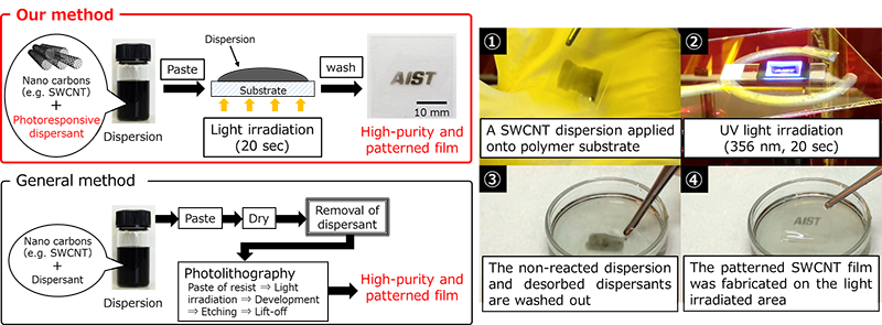
Outline of the developed technology (right) and comparison with conventional technology (left) |
The researchers have developed a special dispersant that selectively adsorbs to nano-carbon materials and desorbs when exposed to ultraviolet light. When irradiated with LED light for a short time (about 20 seconds), single-walled carbon nanotubes (SWCNTs) deposited only on the part exposed to light, and a high-purity thin film only a few tens of nanometers thick was formed. In the conventional wet processes, it was difficult to form a thin film on curved surfaces or uneven surfaces. With the developed technology, it has become possible to prepare a SWCNT thin film on substrates of various shapes and materials including both inorganic and organic materials.
Because existing dispersants are highly adsorptive to nano-carbon materials and are prone to remaining in the thin film of the materials, with conventional methods several complicated steps are necessary including removal of the dispersant with strong acid washing or heat treatment. Furthermore, the remaining dispersant was a factor that lowered electric conductivity. As such, there was demand for a simpler technology to manufacture high-purity nano-carbon thin films which create less of an environmental impact.
With the developed technology, the dispersant does not remain and the processes for thin film forming and patterning are greatly shortened, which will promote the development of next-generation electronic devices, such as flexible and lightweight secondary batteries and capacitors that take advantage of the characteristics of nano-carbon materials.