Takahiro Mori (Researcher) of the New Materials and Devices Integration Group, the Nanoelectronics Research Institute (Director: Tetsuji Yasuda), the National Institute of Advanced Industrial Science and Technology (AIST; President: Ryoji Chubachi), and others have developed a new polycrystalline film-forming technology to achieve a three-dimensional (3D) stacking technology for large-scale integrated circuits (LSIs), greatly improving the performance of N-type polycrystalline germanium (Ge) transistors.
Polycrystalline Ge can be formed at a lower temperature (500 °C or below) than the widely used polycrystalline silicon (Si). This allows CMOS circuits to be directly stacked onto integrated circuits without causing thermal damage, which is promising as an elemental technology for 3D-LSI. In addition, the mobility of electrons and holes in Ge is higher than in Si, so high-speed operation and low-voltage operation are expected. N-type and P-type transistors are required for integrated circuit operations. P-type transistors of polycrystalline Ge have already achieved sufficient performance approaching that of conventional single-crystalline Si transistors. However, the driving current of N-type transistors is lower than that of conventional Si transistors by 10 times or more, which was an issue. The developed technology increased the driving current approximately 10-fold over that of the conventional technology, so the operating speed of polycrystalline Ge integrated circuits is expected to be at the level required for practical use and to contribute to the realization of 3D-LSI devices.
The details of the developed technology will be announced at the “2014 International Electron Device Meeting” to be held in San Francisco, U.S.A. on December 15-17, 2014 (U.S. Pacific Standard Time).
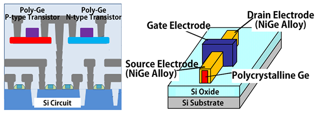 |
Conceptual diagram of a 3D-LSI using polycrystalline Ge transistors (left)
and schematic diagram of the structure of the developed polycrystalline Ge transistor (right) |
In these days, many people have IT devices such as smartphones and tablets, and the amount of processed information has dramatically increased. While further improvement in the information processing capability of IT devices is desired, the amount of power they consume is increasing, so providing ultra-low power consumption to these IT devices is important in promoting a society that consumes less energy. While high performance and low-power consumption of LSIs have been accomplished through miniaturization of transistors so far, further miniaturization has proven technologically and economically challenging. Meanwhile, 3D integrated circuits in which multiple LSIs have been stacked provide not only high integration and high performance without the need for miniaturization technology, but also energy-saving benefits by reducing wire delay. A means of creating thin films of individually created LSIs and stacking them has been developed but is costly and does not sufficiently improve wiring density. It is therefore desirable to have a novel 3D-LSI technology that forms CMOS circuits so as to stack them continuously in a wiring layer of CMOS integrated circuits and connect them to the upper and lower wires.
Together with Tsutomu Tezuka (Specified Concentrated Research Specialist), Koji Usuda (Specified Concentrated Research Specialist) (both currently with Toshiba Corporation), and others of the New Material/New Structure CMOS Development Group, the collaborative research team Green Nanoelectronics Center (GNC) established in the Nanoelectronics Research Institute of AIST had, by the end of March 2014, conducted collaborative research related to P-type and N-type MOSFET using polycrystalline Ge (AIST Press Release on December 12, 2013). This research was aimed at developing higher-performing LSIs that consume less power. Through the present research, new production processes were introduced, leading to the development of N-type polycrystalline Ge transistors with even higher performance.
This research was conducted (FY2010 to FY2013) at GNC with aid from the Funding Program for World-Leading Innovative R&D on Science and Technology of the Japan Society for the Promotion of Science, a system designed by the Council for Science and Technology Policy.
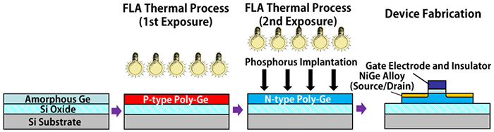
A polycrystalline Ge film that forms transistors is formed as follows: a thermal oxide layer (SiO2) is formed on a Si substrate, then the spattering method is used to deposit an amorphous Ge film that is then crystalized by thermal processing using flash lamp annealing (FLA). When this polycrystalline Ge film is used to form a transistor, the temperature used in processes following thermal processing is a maximum of 350 °C, without causing damage, even if an integrated circuit including copper wires exists on the substrate. The prototype transistor has a junction-less transistor structure with the fin shape shown in the diagrams in the summary (conceptual diagram and schematic diagram of structure). The channel and source/drain parts of a junction-less N-type transistor must all be of the N-type. However, because polycrystalline Ge is usually P-type, it was necessary to convert the polycrystalline Ge layer to N-type, while retaining quality. To do this, after the first heat processing by the FLA method, N-type impurities (phosphorus) were implanted, and FLA was performed a second time to activate these impurities (Fig. 1). This two-step FLA method was able to produce a high-quality N-type polycrystalline Ge film.
 |
|
Figure 1: Process for producing an N-type transistor using the two-step FLA method |
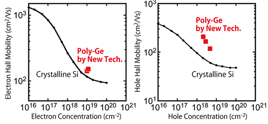
The Hall effect mobility representing the quality of the polycrystalline Ge film produced by this method is shown in Fig. 2. Both the N-type (electrons) and P-type (holes) polycrystalline Ge films had mobility that surpassed that of single-crystalline Si. This shows that a transistor with properties superior to single-crystalline Si could be created using a polycrystalline Ge film formed by the developed method.
 |
|
Figure 2: Hall effect mobility of the polycrystalline Ge produced by the developed method |
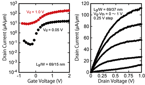
A junction-less N-type polycrystalline Ge transistor (gate length: 70 nm) was produced by processing the N-type polycrystalline Ge film described above into a fin shape and additionally forming a nickel-geranium alloy (Ni-Ge alloy) in the source and drain regions. The transfer and output characteristics are shown in Fig. 3. The drain current value at an operating voltage of 1 V approached nearly 120 µA/µm, a value approximately 10 times greater than the conventional value and equivalent to a polycrystalline Si N-type MOSFET of almost the same size. It is believed that the two-step FLA method improved the activation rate of the impurities over the conventional value, decreasing parasitic resistance. The developed technology markedly improved the operating speed of the N-type transistor, previously considered to be the “bottleneck” of integrated circuit operation of polycrystalline Ge transistors. Polycrystalline Si transistors, which tend to be compared to polycrystalline Ge transistors, generally have poorer performance than single-crystalline Si transistors. The performance of P-type polycrystalline Ge transistors already surpasses that of polycrystalline Si transistors and is on par with that of single-crystalline Si transistors. The developed method thus made great progress toward the realization of high-performance Polycrystalline Ge CMOS circuits.
 |
|
Figure 3: Transfer characteristics (left) and output charactersitics (right) of the developed N-type polycrystalline Ge transistor |
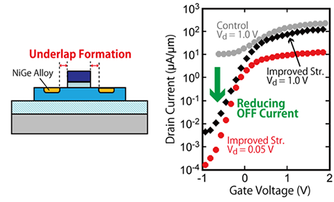
In the transmission properties in Fig. 3, the off-state current is large, so the on/off ratio when 1 V was applied was only about 10, which was problematic. Therefore, in order to reduce the off-state current, a structure providing spaces between the Ni-Ge electrodes and the gate was introduced, reducing the off-state current to 1/1000 (Fig. 4). While the on-state current decreased slightly, a high on-state current and low off-state current can be expected by optimizing the spaces between the Ni-Ge electrodes and the gate.
 |
|
Figure 4: Schematic diagram of the structure of the improved device (left) and its transfer characteristics (right) |
Future plans include forming an integrated circuit combining P-type and N-type polycrystalline Ge transistors onto an insulating film and verifying circuit operation. Further goals include developing a 3D-LSI with stacked polycrystalline Ge in order to greatly miniaturize the LSI, increase performance, and decrease power consumption.