Shin Horiuchi (Chief Senior Researcher) and others of Nanosystem Characterization Group, the Nanosystem Research Institute (Director: Tomohiko Yamaguchi), the National Institute of Advanced Industrial Science and Technology (AIST: President: Tamotsu Nomakuchi), have found that when a metal thin film formed by electroless plating on a plastic substrate is irradiated for a very short time with high-intensity pulsed light, the adhesion of the plated film to the substrate is dramatically improved without damage of the substrate. This technology also provides a simple patterning technique of the plating film.
Electroless plating has been widely used in industries to produce metal thin films on insulating materials such as plastics products with complex shapes for electronic and automotive parts. Generally, in metal-film forming, the surface of the substrate must be pre-treated to produce roughness (e.g. by plasma processing or chemical etching) to enhance the adhesion to the substrate. In electroless plating, in particular, it is difficult to ensure sufficient adhesion without such pre-treatment.
In the developed technology, a plated film formed without surface treatment of the substrate is irradiated with high-intensity pulsed light for a very short time (several hundred microseconds), causing instantaneous heating of the metal film to a high temperature. As a result, only the interface between the plated film and the plastic substrate can be heated, thus increasing the film adhesion without the damage of the substrate. A large (A4-size) plating film can be treated in a very short time (order of microseconds). In addition, the irradiation of the pulsed light through a photo mask allows us to produce metal patterns on plastic films. That is, the masked region remains poor in adhesion and can be easily peeled off with adhesive tape.
Electroless plating is a wet chemical film-forming process to form metal films on insulating materials, such as plastics, glass and ceramics, and has been used in various industries including electronics (e.g. printed circuit boards) and automotive (e.g. wheel caps and steering wheels) industries. Unlike physical dry film-forming processes such as sputtering, which requires an expensive vacuum system, electroless plating is an inexpensive process and thus has been used in a wide variety of applications to form films of copper, nickel, gold, and other metals.
Conventional electroless plating requires surface roughening to improve adhesion. The surface is roughened by using a physical process such as plasma processing which uses a vacuum system or a chemical etching process using hazardous oxidizing chemicals. However, these processes have some problems. For example, if the surface of the substrate is roughened, the metal thin film formed on the surface is not smooth and the electrical and optical characteristics of the film are adversely affected. Moreover, to form a fine conductive pattern, the metal plating film is formed over the entire surface of the substrate, a mask pattern is formed on the film with a photoresist, and then the metal film is etched. This process includes several steps which produce a large amount of waste causing a high environmental load, as does the etching process.
AIST has discovered a technique for immobilizing, on a plastic surface, nanoparticles of noble metals such as palladium and platinum, which act as catalysts for electroless plating (AIST press release on September 18, 2008). AIST is developing an etchingless electroless plating process that ensures high adhesion without roughening the surface of the substrate. In collaboration with Satoru Shimada (Senior Researcher) and others of Mesoscopic System Group, the Electronics and Photonics Research Institute (Director: Satoshi Haraichi), AIST, the researchers are studying film-formation processes that use high-intensity pulsed light. In the present research, the researchers have integrated the above-mentioned research activities to improve plating-film adhesion and develop simple plating-film patterning using a photo mask.
The results of this research have been obtained as part of “Research on an Advanced High-Adhesion Etchingless Electroless Plating Process”, a project of Adaptive and Seamless Technology Transfer Program through Target-driven R&D (A-STEP) of Japan Science and Technology Agency.
In electroless plating, a metal thin film is formed by chemical reduction of metal ions in the solution after immobilizing the catalyst on the surface of the substrate. In this research, platinum colloid, uniform 3-nm polymer-covered platinum nanoparticles stably dispersed in water, is used as the catalyst. When a substrate such as plastics is immersed in the platinum colloid, the platinum nanoparticles are uniformly immobilized on the surface of the substrate. Then, when the substrate is immersed in a mixed aqueous solution of low-concentration hydrogen peroxide and tetrachloroauric (III) acid, catalysis by the platinum nanoparticles causes hydrogen peroxide to reduce tetrachloroauric (III) acid (see the formula below), and a gold plating film about 100 nm thick is formed:

Conventionally, the substrate is annealed for about 30 minutes at 100 to 250 ℃ after plating. (The temperature varies depending on the properties of the substrate.) As a result, the adhesion of the plating film is improved, and a gold plating film is formed that does not peel off in a “Scotch-Tape test” in accordance with JIS K5600-5-6. In this process, the surface is not roughened and the adhesion of the plating film is improved by annealing after plating. Copper, nickel, and platinum plating can be performed in a similar way using palladium colloid as the catalyst. However, post-plating annealing can cause problems such as warping and deformation of the substrate, and takes 10 to 30 minutes.
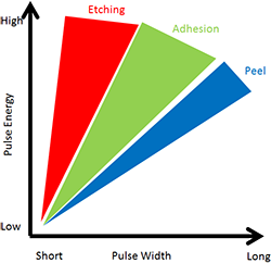
The researchers investigated a post-plating process that uses high-intensity pulsed light as an alternative to the conventional annealing process. When a plating film formed on a plastic substrate is irradiated with several hundred microseconds of pulsed light, only the interface between the plating film and the plastic substrate is heated instantaneously. Consequently, the adhesion of the plating film is improved and changes such as warping and deformation do not occur to the substrate. Figure 1 shows the conditions of pulsed-light irradiation and post-irradiation conditions (adhesion, removal, peeling) of a gold plating film on a polyethylene terephthalate (PET) film. When the film was irradiated once with 300 µs and 1.21 J/cm2 of pulsed light, the adhesion was improved so that the film did not peel off in a tape-peeling test. When it was irradiated once with pulsed light with higher energy (e.g. 300 µs and 2.06 J/cm2), the plating film was removed (etched). When the film was irradiated with pulsed light of lower energy (blue in Fig. 1), the adhesion was not improved and the film peeled off easily in a tape-peeling test.
 |
|
Figure 1: Changes in the adhesion of a gold plating film on a PET film under different conditions of pulsed-light irradiation (irradiation time and intensity) |
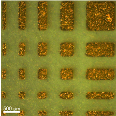
To determine whether a metal pattern, such as a wiring pattern, could be formed by irradiation with pulsed light, a photo mask with a specified pattern printed on a PET film with a laser printer was placed on a gold plating film and the film was irradiated once with 300 µs and 1.21 J/cm2 of pulsed light. The adhesion of the plating film was poor in the areas that were masked and not exposed to the light. Adhesive tape was attached to these areas and peeled off. The film peeled off with the tape, leaving the gold metal pattern on the substrate. When the energy of the pulsed light was increased, the exposed areas of the film were etched and a reverse pattern was formed. It was confirmed that adhesion improvement and etching with pulsed light are possible on various plastic substrates. A metal micro-pattern (Fig. 2) can be formed by using a photo mask with the micro-pattern.
 |
|
Figure 2: Gold-plated micro-pattern on a PET film |
The developed electroless plating process can be applied to other metal plating films and various plastic substrates. AIST is in the process of transferring this electroless plating technology to businesses in areas affected by the Great East Japan Earthquake. The researchers will collect data on the pulsed-light irradiation conditions effective for different combinations of metals and plastics and will develop applications of this technology, taking into account the needs of earthquake-affected businesses. Because this phenomenon is specific to plating films and its effects on metal films formed by other processes such as sputtering are not the same, the researchers intend to investigate the mechanism behind it.