- First-ever success in evaluating molecules within a sealed organic light emitting diode device in operation -
Takayuki Miyamae (Senior Researcher), Nanosystem Characterization Group, the Nanosystem Research Institute (Director: Kiyoshi Yase) of the National Institute of Advanced Industrial Science and Technology (AIST; President: Tamotsu Nomakuchi), and Noriyuki Takada (Leader), Printed Electronics Device Team, the Flexible Electronics Research Center (Director: Toshihide Kamata) of AIST, have developed a method that can selectively measure the behavior of specific molecules at the interfaces of organic layers in a multilayered organic light emitting diode (OLED) device during light emission in collaboration with Chemical Materials Evaluation and Research Base (CEREBA; President: Ryuichi Tomizawa). The researchers have succeeded for the first time in measuring the behavior of the electric charges in a device at the molecular level.
The developed method uses an advanced laser spectroscopic technique that has been improved to measure the molecular vibrational spectrum at the interface of a specific organic layer inside an OLED device. By employing a signal enhancement phenomenon that occurs at the interface with a concentrated electric field, the method can be used to evaluate the molecular condition of the organic layer during light emission without destroying the device. This world-first has been achieved through the merger of AIST’s cutting-edge fundamental measurement technology with CEREBA’s practical OLED device manufacturing and evaluation technologies.
The method is expected to be useful for elucidating the deterioration of materials and deterioration of interfaces in a device on the basis of molecular level information. Such elucidation is necessary for extending the life of OLED devices.
Details of this technology will be published online in Applied Physics Letters, an American scientific journal, on August 15, 2012 (EDT). They will also be presented at the 73rd Japan Society of Applied Physics Autumn Meeting 2012 to be held at Ehime University and Matsuyama University (Matsuyama, Ehime) from September 11 to 14, 2012, and at the 6th Annual Meeting of the Japan Society for Molecular Science to be held at the University of Tokyo (Bunkyo, Tokyo) from September 18 to 21, 2012.
 |
|
(Figure) : Conceptual diagram of laser spectroscopy of a multilayered OLED device during light emission |
In recent years, the application of OLED devices, which have the superior properties including a wide viewing angle, low-voltage operation, and video playback capacity, to equipment such as next-generation flat screen televisions, smartphones, and lighting has attracted much attention. As practical OLED devices with high brightness and long life, multilayered OLED devices composed of multiple organic layers, each with different properties, are used. These OLED devices are tightly sealed with a desiccant to eliminate the most serious causes of OLED device deterioration, namely, the effects of oxygen and water. Therefore, the only means of gaining access to the OLED device itself is via the electrode connected to it or via the transparent window used to let light pass through. However, because of the hindrance by the fluorescent light emitted by the organic materials and the strong light emitted when the device is in operation, most evaluating and measuring methods that use light are very difficult to use. The only available methods for examining degradation behavior are indirect and limited: for example, electrical properties of the operating device are examined and then a model analysis is conducted or the device is destroyed and then the insides are analyzed. If a method that requires destruction of the device is used, the effects of the destruction and of contamination by impurities cannot be completely eliminated. Moreover, when an unsealed device is used, degradation due to external factors such as water occurs at the same time and it is difficult to isolate and evaluate intrinsic degradation at a molecular level. Because of these difficulties, the mechanism of the slow degradation that occurs when OLED devices are in operation for long hours remains unknown even after more than 25 years since the structure of the current OLED devices was proposed. In addition, in the case of practical-level multilayered OLED devices, the information from multiple organic layers becomes overlapped and inseparable, making it extremely difficult to separately evaluate the behavior of each organic layer and its relationship to degradation. Extension of the life of multilayered OLED devices is the key to their practical application to high-definition displays or lighting. For this purpose, the non-destructive acquisition of information on what is happening in each layer of the device during its long hours of operation and on how the events in each layer trigger device degradation has been a pressing agenda. To achieve these goals, nondestructive evaluation and measurement methods that can be used to measure the state of each organic layer in sealed, multilayered OLED devices in operation has been desired.
AIST has been developing a technique for evaluating and analyzing the interfaces of organic substances by using sum frequency generation (SFG) spectroscopy to selectively measure and evaluate molecular information on material surfaces and interfaces. In addition, with the aim of practical application to the evaluation of organic electronic materials and practical devices, AIST has also been pursuing the development of two-color SFG spectroscopy that uses wavelength-tunable lasers in order to collect information on specific interfaces of organic substances in organic devices with complex structures.
CEREBA was established at AIST as a research and development base for evaluation to contribute to timely product development through the development and sharing of evaluation and analysis techniques for next-generation chemical materials. With its focus on organic electronic materials (especially on OLED materials), CEREBA has been pursuing the establishment of design and manufacturing technologies for a standard device which will become a unified evaluation standard applicable to practical OLED materials and devices that do not yet have established evaluation methods. CEREBA also aims to develop evaluation and analysis techniques based on these technologies.
This research and development has been supported by Grants-in-Aid for Scientific Research (basic research) of the Japan Society for the Promotion of Science and carried out as the Next Generation Green Innovation Evaluation Base Technology Development (FY2010-2015) commissioned by the New Energy and Industrial Technology Development Organization.
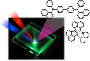
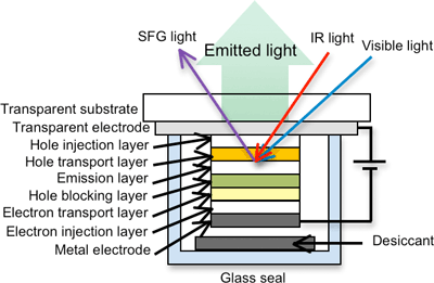
OLED devices are composed of stacked organic layers with different properties sandwiched between two electrodes. The device emits light when a voltage is applied to the electrodes. In ordinary multilayered OLED devices, between three and five organic layers are stacked on a transparent electrode with an overall thickness of only about 200 nm. To eliminate the influence of oxygen and water, the device is tightly sealed with a desiccant (Fig. 1). The multilayered OLED device used for the measurement was composed of six different organic substances and had a brightness half-life (the length of time required for the brightness to deteriorate to 50% of the initial value) of more than 13,000 hours at brightness of 1000 cd/m2 (candelas per square meter).
The developed method is an evaluating and analyzing technique using SFG spectroscopy that uses infrared laser light and visible laser light. By using the SFG spectroscopy, the vibrational spectrum of molecules at the surface and at the interfaces in a solid can be measured. Normally, the wavelength of the visible laser light in SFG spectroscopy cannot be changed, but two-color SFG spectroscopy that can change the wavelength of the visible laser light is used so that a phenomenon called a double resonance effect can be utilized. In this effect, the wavelength of the visible light is adjusted to match the absorption wavelength (color) of the target organic substance, thus allowing only the target organic substance to be selectively brought to a high-energy state. The use of this double resonance effect makes it possible to eliminate the influence of other organic layers within the device and to enhance and isolate the signals from the target organic layer. In addition, to minimize damage that could be caused to the device by the laser light, improvements were made to the SFG spectrometer so that it could maintain its measurement resolution even when the laser power was reduced to less than 1/100 of that in conventional SFG spectrometers. Figure 1 shows the structure of an actual multilayered OLED device. The visible and infrared laser lights used in SFG spectroscopy were incident from the transparent substrate side when measurements were made. Even though an operating OLED device emits strong light, the SFG light has a different wavelength from the emitted light. Moreover, because the beam-like SFG light is emitted in a certain direction, a filter and two spectrometers were used to clearly separate the SFG light from the strong emitted light and then measure it.
 |
|
Figure 1 : Schematic drawing of the structure of the multilayered OLED device and the directions of the incident and emitted lights used for SFG spectroscopy |
The SFG spectra of a multilayered OLED device in operation are shown in Fig. 2. A typical multilayered OLED device using the phosphorescence of iridium complexes is used in this measurement. If the absorption wavelengths of organic substances were close to each other, the signals from multiple organic layers would be collected simultaneously. Introduction of a tunable visible laser alone cannot avoid such a situation. As shown in Fig. 2, the signals from multiple organic layers are observed together without voltage application (see the spectrum in Fig. 2 left middle). On the other hand, when the device is in operation with applied voltage, a spectrum that is clearly different from that under no applied voltage is measured (see the spectrum in Fig. 2 left top). Moreover, when the voltage applied to the device is changed, a change in signal strength is clearly observed.
This developed method makes use of an effect called a field-induced effect. When an electric field is applied to a sample, the SFG signal from the organic layer that responds to the electric field is strengthened. In an OLED device with multiple stacked organic layers, an energy difference between adjacent organic layers exists in some interfaces because of differences in the ionization potential or electron affinity of the organic substance. The electric charges that move around in the operating OLED device are accumulated near the interfaces that have an energy difference. The accumulated electric charges then create a localized electric field and allow only the SFG signal from the organic layer with the accumulated electric charges to be selectively observed.
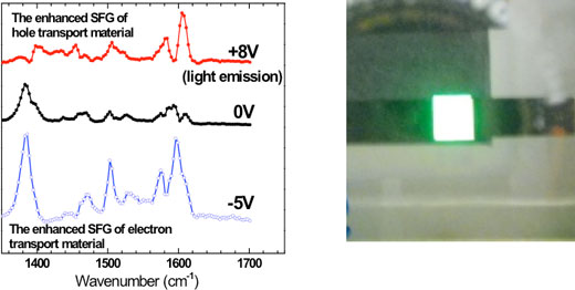 |
Figure 2 : Spectral changes in an operating multilayered OLED device
(Left) starting from the top, with +8 V application (light emission), no voltage application, and -5 V application
(Right) Photograph of an OLED device emitting light with voltage application |
The spectrum that is intensified in response to the voltage matches the spectrum of the organic substance of the hole transport layer. This spectral behavior can be explained by the fact that when the device is in operation, owing to the energy difference between the hole transport layer and the light emitting layer, electric charges are accumulating near the interface of these two layers. It has been revealed for the first time that electric charges are accumulated at the interface of the hole transport layer in an operating OLED device. In contrast, when a reverse voltage is applied to this device the vibrational spectrum of the hole transport layer disappears and the vibrational spectrum (Fig. 2 left bottom) of an organic substance in the electron transport layer appears instead. By using two-color SFG spectroscopy on a sealed, multilayered OLED device in operation with the same structure as a practical OLED device, and by making use of the field-induced effect that occurs when various voltages are applied to the device, the information on each organic layer and the location of the accumulated electric charges, which cannot be measured so far, can be measured directly without destroying the device. This new method is applicable to the evaluation and degradation analysis of organic electronic devices.
The frequency pattern in a vibrational spectrum is sensitive to the state of molecules. Even molecules of the same species in different condition will result in differences in frequencies and the change in molecular orientation in a layer will lead to changes in intensity. For these reasons, a frequency pattern is like a “fingerprint” unique to each molecule. By investigating in detail the “fingerprints” of organic layers in an OLED device, the alteration and degradation of molecules in the operating device as well as the change in the electric field inside the device can be elucidated. Now that the molecular status and electric charge distribution in operating devices can be revealed, it will be possible to closely examine how these things change when the device has been in operation for a long time. It is expected that valuable information will be acquired to further improve the properties of OLED devices and address the unsolved problem of degradation.
For OLED devices to be applied to next-generation flat screen televisions, smartphones, and flexible devices, the degradation progressing in practical devices must be investigated in detail. Using the developed method, the researchers plan to continue to investigate the molecular-level status in operating OLED devices and in devices that have been in operation for long hours. They aim at the molecular-level elucidation of the driving mechanism of OLED devices and the degradation mechanism of them which is indispensable to the extension of device life.
The researchers also aim to apply the method to the evaluation and analysis of other organic electronic devices such as organic solar cells and organic transistors.