Sei Uemura (Researcher), Printed Electronics Device Team, the Flexible Electronics Research Center (Director: Toshihide Kamata) of the National Institute of Advanced Industrial Science and Technology (AIST; President: Tamotsu Nomakuchi), has developed an all-printed flexible pressure sensor in collaboration with Ajinomoto Co., Inc. (Ajinomoto; President: Masatoshi Ito).
AIST and Ajinomoto have developed a polyamino acid material that exhibits piezoelectricity and have fabricated a sensor array printed on a flexible substrate by forming the material into an ink and adopting a structure that reduces current leakage. This fabrication technology by printing for the sensor array, as well as the increased sensor array size, will allow affordable sensors to be supplied in large quantities. This technology is expected to contribute to the widespread use of sensor network devices such as watch sensors.
Details of this technology will be presented at the 42nd International Electronic Circuits Exhibition (JPCA Show 2012) at Tokyo Big Sight, Koto-ku, Tokyo from June 13 to 15, 2012.
 |
|
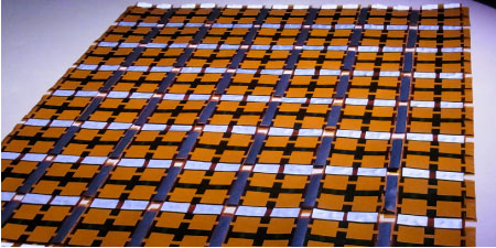
All-printed flexible pressure sensors |
In recent years, sensor networks through which people can communicate with electronic devices from anywhere and at any time have been attracting attention to create a safe and secure society. There is an expectation that a system will be developed in which unobtrusive sensors will provide the necessary information, such as movement of people, to the network. These sensors need to be applicable to a wide variety of uses, affordable, and mass-producible. Existing pressure sensors are very expensive and often not suitable for array fabrication. Also, the structures of these sensors make it difficult to increase the sensor array size, preventing their widespread use in society.
AIST has been conducting research and development of flexible electronic devices. Particularly, it aims to develop a technology to perform all fabrication processes by printing and has developed an all-printed memory array, an RF tag, an evapotranspiration sensor, etc. Ajinomoto has years of experience in research and development of functional organic materials, such as amino acids and polyamino acids, and in the production technology of them.
The all-printed memory arrays developed by AIST are ferroelectric memory arrays that use ferroelectric polyamino acids as the ferroelectric layer of the transistor. The polyamino acids exhibit high ferroelectricity as well as high piezoelectricity when the large dipole moment of the main chain is efficiently used. AIST and Ajinomoto have developed a polyamino acid material suitable for piezoelectric devices and have fabricated a pressure sensor array by forming the material into an ink and adopting a device structure suitable for printing processes.
◊Development of a new polyamino acid piezoelectric material
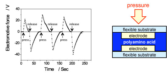
When a polyamide acid material, which has a rigid rod-like molecular structure called an α-helix, is applied to the substrate to form a film, the rod-like structure acts as the mesogen and the molecular axes are aligned in parallel with the substrate surface (Fig. 1). The film exhibits ferroelectricity and ferroelectric memory devices have been fabricated using this ferroelectricity. To use the film as a piezoelectric material, it is important to increase the amount of pressure-induced polarization, in addition to the regular alignment. The molecular design of the piezoelectric polyamino acid suitable for the device was implemented to increase the dipole moment of the main chain along the molecular axis of the polyamino acid, as well as to make it soluble and thus form it into an ink. The polyamino acid synthesized by following this molecular design exhibited a voltage of several tens of volts when a load of 6 kg was applied to an area of 10 cm2 (Fig. 2).
 |
|
Figure 1 : Structure of the main chain of polyamino acids |
 |
|
Figure 2 : Device cross-section (left) and the voltage generated when pressure was applied (right) |
◊Use of a structure suitable for printed devices
An example of the simplest structure of flexible electronic devices is shown as the device cross-section in Fig. 2. An electrode is formed on a flexible substrate and a thin layer such as a ferroelectric layer is then printed on it. A second electrode is then printed directly on the thin layer or otherwise a flexible substrate on which an electrode is already printed is placed on the thin layer. However, even with such a simple structure it is difficult to form the device by printing. With the developed flexible piezoelectric sensor, a piezoelectric layer is sandwiched between two silver electrodes screen-printed on plastic substrates. To fabricate the sensor by printing, the piezoelectric layer would need to be formed on the bottom electrode. However, because of the large irregularities in the surface of the printed electrode and the difficulty in precisely forming a three-dimensional shape, formation of the ferroelectric layer on the electrode is strongly affected by the electrode surface, making it difficult to form a high-quality thin layer. In this research, it was difficult to completely cover the screen-printed bottom electrode, which is about 50 µm thick, with the piezoelectric layer. Thus, a large leak current occurs when the top electrode comes into contact with the bottom electrode. To prevent the current leakage, the piezoelectric layer needs to be made thicker and the voltage required to drive the sensor has to be increased considerably. Owing to the marked effect of the leak current at the edge of the bottom electrode, it is necessary to ensure that the edge is insulated. A new structure was adopted to prevent current leakage at the edge of the bottom electrode and a thin piezoelectric layer has become usable. As a result, the leak current has decreased to an acceptable level and the yield of the device has increased from a few percent to nearly 100 %.
◊Joining method suitable for sheet devices
There are two methods for increasing sensor array size: by forming a sensor array directly onto a large substrate and by forming the sensor array onto small, multiple substrates and then joining the substrates together. Although the former is suitable for mass production of the same device, the latter has advantages such as equipment downsizing and enabling different devices to be arbitrarily arranged to meet a wide variety of needs.
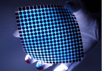
In this research, the method of joining substrates to increase the array size was used (Fig. 3). The pressure sensor is subjected to pressure from above the device and requires enough joining strength to withstand this pressure. Although an adhesive has been conventionally used to join the flexible substrates together, a technology to structurally increase the strength of the joints between the substrates has been developed.
 |
|
Figure 3 : The large-area pressure sensor array (80 cm long, 80 cm wide) |
The researchers intend to enhance the performance of the piezoelectric sensor, including the improvement in its sensitivity and the miniaturization of it. They will also propose new applications of piezoelectric sensor devices by developing combinations with other devices and network interfaces. Because the developed piezoelectric sensor array can be used for vibration power generation, they aim to develop self-power-generating sensors by combining the array with a battery.