- Technology for transferring single-crystal germanium layers to various substrates -
Tetsuji Yasuda (Leader), Tatsuro Maeda (Senior Researcher), Taro Itatani (Senior Researcher), and others of New Materials and Devices Integration Group, the Nanoelectronics Research Institute (Director: Seigo Kanemaru) of the National Institute of Advanced Industrial Science and Technology (AIST; President: Tamotsu Nomakuchi), have developed a fabrication technology for germanium (Ge) platform substrates in collaboration with Sumitomo Chemical Co., Ltd. (Sumitomo Chemical; President: Masakazu Tokura).
This research makes use of the strengths of AIST’s substrate bonding and device manufacturing technologies and Sumitomo Chemical’s crystal growth technology. In order to achieve practical application of high-quality Ge platform substrates, three technologies have been developed: (1) a technology for the epitaxial growth of a high-quality Ge and aluminum arsenide (AlAs) layers on a gallium arsenide (GaAs) substrate; (2) a peeling-off technology for a thin-film Ge layer using the epitaxial lift-off method; and (3) a technology for bonding a high-quality thin-film Ge layer to an arbitrary substrate.
The developed technology is expected to contribute to the development and function integration of new devices based on Ge by combining electronics and photonics.
Details of this technology will be presented at the 2011 International Conference on Solid State Devices and Materials (SSDM 2011) to be held in Nagoya, Japan from September 28 to 30, 2011.
 |
|
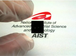
A thin film of high-quality single-crystal germanium (10 x 10 mm) on a glass substrate (18 x 18 mm) |
Ge is used as a material for photonic devices and high-efficiency solar cells. In addition, recently active research efforts are underway to use Ge as a promising channel material in post-silicon high-performance transistors, and Ge is also attracting attention as a new platform substrate material for fusing electronics and photonics. Because single-crystal Ge substrates are expensive and fragile, high-quality single-crystal Ge layers on substrates made of inexpensive and easy-to-handle materials such as silicon, glass, and plastic have been strongly demanded.
AIST and Sumitomo Chemical have promoted joint research to develop hybrid semiconductor technology since 2008, and have conducted fundamental research to fuse silicon-based high-performance semiconductor chips with Ge and III-V semiconductor devices that have various functions as photonic materials. The present research makes use of AIST’s world-class Ge device manufacturing technology and Sumitomo Chemical’s epitaxial growth technology for Ge and III-V semiconductors with commercial quality, and succeeded in manufacturing high-quality Ge platform substrates suitable for the integration of various device functions.
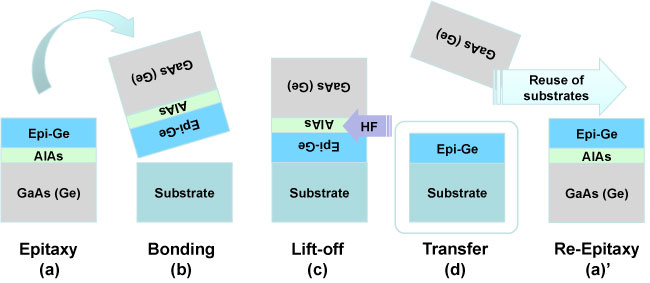
Figure 1 shows the newly developed Ge platform substrate manufacturing method. First, a high-quality Ge layer (Epi-Ge) is epitaxially grown on a GaAs or Ge substrate, with an AlAs layer between the Ge layer and the substrate. Owing to good lattice matching of Ge, GaAs, and AlAs, a high-quality single-crystal Ge layer can be easily obtained (Fig. 1(a)). Next, the substrate with the high-quality Ge layer is bonded with arbitrary substrates such as silicon, transparent glass, or plastic (Fig. 1(b)). Then, the GaAs or Ge substrate is peeled off by selectively dissolving the AlAs layer with a hydrofluoric acid (HF)-based solvent (Fig. 1(c)). Eventually, the high-quality thin-film Ge layer is transferred to the arbitrary substrate (Fig. 1(d)). This method is called the epitaxial lift-off (ELO) method, and has the advantage that the expensive GeAs (Ge) substrate can be reused after peeling (Fig. 1(a)’).
 |
|
Figure 1 : The transfer method for a high-quality Ge layer |
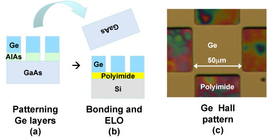
Figure 2 shows examples of high-quality Ge layers transferred to a transparent glass substrate and a flexible plastic substrate. The Ge layer area is 10 mm x 10 mm, which is large enough for use in manufacturing and integrating various chips and devices. In addition, high-quality Ge layers with patterns in 100 µm or finer level have also been transferred (Fig. 3). These results indicate that the Ge ELO technology enables us to obtain high-quality Ge layers on any substrate and any place with any pattern.
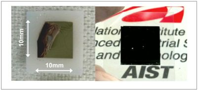 |
Figure 2 : High-quality single-crystal Ge layers on a plastic substrate (left)
and a transparent glass substrate (right) |
 |
|
Figure 3 : Transfer of microfabricated high-quality single-crystal Ge Hall pattern |
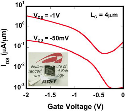
In addition to transferring high-quality Ge layers, the developed technology can also be used to transfer Ge-based devices. Figure 4 shows the characteristics and a photograph of a Ge transistor with a gate length of 4 µm transferred onto a glass substrate. The grown Ge layer shows a sufficient quality for good device operations, and the electrical characteristics do not change even after transfer to the glass substrate, revealing the effectiveness as a device transfer technology. This technology can be applicable to manufacture various devices such as Ge transistors and Ge-based solar cells on growth substrates, and to arrange layer multiple devices on an arbitrary substrate as necessary, enabling integration and mixing with conventional devices.
 |
|
Figure 4 : Electrical characteristics and a photograph of a Ge transistor with a gate length of 4 µm transferred onto a glass substrate |
Various Ge-based devices are currently used in a wide range of fields. The developed Ge ELO technology will create new applications of Ge-based devices by supplying various substrates with high-quality single-crystal Ge layer and transferable Ge devices. The technology will also contribute to the unprecedented integration, such as the fusion of electronic and photonic devices into a single chip, and the weight reduction of solar cells. In the future, Ge platform substrates for these applications will be supplied.