Shigeki Sakai (Leader) et al. of the Novel Electron Devices Group, the Nanoelectronics Research Institute (Director: Seigo Kanemaru) of the National Institute of Advanced Industrial Science and Technology (AIST) (President: Hiroyuki Yoshikawa) in collaboration with Ken Takeuchi, Associate Professor of the Graduate School of Engineering, the University of Tokyo (Univ. Tokyo) have demonstrated that the use of ferroelectric gate field-effect transistors (FeFETs) as memory cells dramatically improves the performance of NAND flash memory. The FeFET, the newly developed memory cell, can be programmed and erased as many times as 100 million or more and with programming voltage of less than 6 V, whereas the conventional NAND flash memory cells have ten thousand program/erase endurance cycles with approximately 20 V programming voltage. It has been assumed that conventional NAND flash memory can be downsized to 30 nm at the minimum, whereas this novel memory cell will meet the needs of the next 20-nm and 10-nm technology generations. And thus, this memory cell is expected to be used in a next-generation, high-density, high-capacity nonvolatile memory.
Results of the research was reported at the 23rd Nonvolatile Semiconductor Memory Workshop (the 23rd IEEE NVSMW / the 3rd ICMTD 2008) held in France, May 18–22, 2008.
 |
|
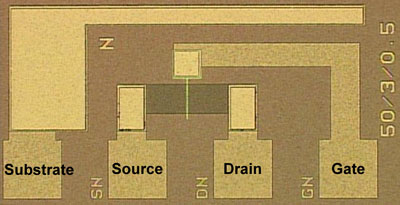
Optical microscopic image of an FeFET for Fe-NAND flash memory. The gate length and width are 3 µm and 50 µm, respectively.
|
As portable information devices have become increasingly widespread in recent years, the need for smaller, lighter and less power-consuming data storage systems of high-capacity is growing. As a high-capacity data storage system, small, light and shock-proof solid state drives (SSDs) based on NAND flash memories have been attracting much attention these days instead of the conventional hard disk drive (HDD) which requires mechanical parts such as a motor. Cost per bit of NAND flash memory is higher than that of the HDDs with magnetic disks. However, with efforts toward lowering the bit cost by increasing the cell density per unit area, the NAND flash memory has rapidly become popular in the market.
The NAND flash memory, however, can be programmed and erased approximately ten thousand times only, and further downsizing for increasing the cell density will reduce the number of the program/erase endurance cycles and degrade the data reliability. It is said that conventional memory cells cannot be downsized below 30 nm process node because further downsizing will cause problems such as capacitance coupling noise between the floating gates of neighboring memory cells.
The realization of using the FeFETs as memory cells in a ferroelectric NAND (Fe-NAND) flash memory will not only dramatically increase the number of program/erase endurance cycles, but also decrease the capacitance coupling noise between neighboring memory cells due to the absence of floating gates. For these reasons, the Fe-NAND is expected to be a high-density, high-capacity nonvolatile memory suitable for the future 20-nm and 10-nm technology generations following the coming 30-nm.
AIST has been working on the development of the FeFET, which is a transistor that can be also used as a memory device. Since the operating principle of the FeFET was first published in 1963, its short data retention time has been a problem to be solved. In 2002, however, AIST succeeded in improving the data retention characteristics very much by using a Pt/SrBi2Ta2O9/Hf-Al-O/Si gate structure, and, in 2004, demonstrated that the FeFET can be downsized following a scaling rule by applying a self-aligned gate technique (press releases of October 2002 and December 2004). Since then, AIST has continued its research toward realizing practical applications of the FeFET in semiconductor integrated circuits. As a part of this effort, AIST has been collaborating with Ken Takeuchi, Associate Professor of Univ. Tokyo, to investigate possible applications of the FeFET in NAND flash memories, partly in cooperation with Takayasu Sakurai, Professor of the Institute of Industrial Science, Univ. Tokyo and Makoto Takamiya, Associate Professor of the VLSI Design and Education Center, Univ. Tokyo.
This research was conducted as a part of the "Development Project of Nonvolatile Logic Circuit Board Technology for Low Power Consumption Processors" under the "Efficient Energy Utilization Basic Technology Pilot Research and Development Project" under the "Strategic Research and Development Project of Efficient Energy Utilization Technology" of the New Energy and Industrial Technology Development Organization.
First, an approximately 10-nm-thick high-permittivity dielectric Hf-Al-O film, 400-nm-thick ferroelectric SrBi2Ta2O9 film, and then 200-nm-thick platinum film were deposited in this order on a p-type Si semiconductor substrate using a pulsed-laser deposition technique. The conditions of impurity doping to the channel area had been adjusted so that the threshold voltage was optimized for a NAND flash memory cell. The gate, source, drain and substrate electrodes were formed using the photolithography. And then, an n-channel FeFET with a metal-ferroelectric-insulator-semiconductor (MFIS) stacked gate structure was obtained (Fig. 1).
An array structure of a Fe-NAND flash memory was assumed to be as shown in Fig. 2, and the appropriate voltage application conditions that enabled the data program, all erase, and readout operations were carefully examined. Threshold voltages of the FeFET were measured after applying program and erase voltage pulses with a variety of pulse widths. The result was that the pulses with high speed of 10 µs and low voltage of 6V worked enough for showing two distinguishable threshold voltages which corresponded to the two different memorized states. The threshold voltages of the FeFET were measured also after applying program and erase disturb voltages which were the voltages inevitably applied on unselected cells at the same time that the selected cells were programmed and erased. As a result, we found out the appropriate voltage application conditions for the unselected cells to avoid memory errors by the program and erase disturbs.
Judging from the extrapolated lines drawn on the threshold-voltage retention curves of the program, erase, and program disturb operations (Fig. 3), this n-channel FeFET was expected to retain the data for as long as ten years. In addition, the threshold voltages did not change significantly even after 100 million voltage pulses of 10 µs and 6 V were applied for both data programming and erasing (Fig. 4), indicating that the FeFET had more program/erase endurance cycles than 100 million times.
In conclusion, we fabricated an n-channel FeFET for use as a memory cell in an Fe-NAND flash memory and demonstrated that the FeFET had more program/erase endurance cycles than 100 million times and less operation voltage than 6 volts. This memory cell is suitable for a high-density, high-capacity nonvolatile memory of 20-nm and 10-nm technology generations, which will not be realized by conventional flash memories.
|
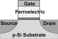
Fig.1 N-channel type FeFET with an MFIS gate stacked structure.
|
|
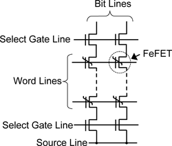
Fig.2 Assumed memory cell array of Fe-NAND flash memory.
|
|
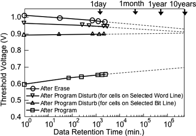
Fig.3 Data retention characteristics of threshold voltages after program, erase and program disturb operations.
|
|
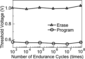
Fig.4 Endurance characteristics.
|
We will pursue the research on downsizing and large-scale integration of the FeFET and will also design and develop the Fe-NAND flash memory array circuits and verify their operations in cooperation with Univ. Tokyo.