- Power Transistor with Ultra-Low Power Loss Reduces Greenhouse Gas Emission by 1 % -
The Power Electronics Research Center (PERC), the National Institute of Advanced Industrial Science and Technology (AIST), an independent administrative institution, has prepared SiC-static induction transistor (SiC-SIT) with buried p+ gate area by using hexagonal silicon carbide (4H-SiC) through an original fabrication process, in collaboration with Kasuga-Yano Laboratory, Interdisciplinary Graduate School of Medical and Engineering, Yamanashi University, a national university corporation (to be designated as Yamanashi U., hereinafter). The new SiC-SIT is characterized by breakdown VBR voltage 700 V and specific on-resistance RonS 1.01 mΩ·cm2, which is the smallest RonS in the world for switching devices of VBR 600 V~1.2 kV class (Figs. 1 and 2). The use of SiC-SIT will reduce the power loss extensively to 1/12 that of silicon insulated gate bipolar transistor (Si-IGBT)
The newly developed buried gate SiC-SIT will cover a broad spectrum of applications ranging from small capacity inverters in household electric appliances energized by commercial AC 100/200 V line (e.g. induction heating (IH) cooking heater, air-conditioner, eco-friendly hot water supply) and uninterruptible power source (UPS); medium capacity inverters in electric vehicles (hybrid car, battery-driven car, fuel cell-driven car, and so on) to large capacity inverters for the control of large motor in the industrial area, as well as distributed power source system and photovoltaic power generation. The market size is expected to surpass 1 trillion yen. According to a tentative estimation, the practical application of SiC-SIT in these areas will reduce the carbon dioxide emission as of 2020 in Japan to 1 % of total emission in 1990, contributing to the reduction of greenhouse gas (carbon dioxide) emission as required by the Kyoto Protocol having been put into effect on February 16, 2005.
Details of the present work will be reported at the 52nd Joint Meeting of the Japan Society of Applied Physics and Related Academic Circles to be held from March 29 to April 1, 2005 at the Saitama University.
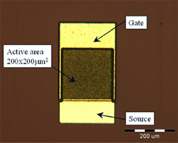
Fig. 1 Construction of newly developed buried gate SiC-SIT device
|
|
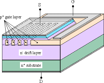
Fig. 2 A schematic diagram of newly developed buried gate SiC-SIT device
|
Silicon carbide (SiC) is characterized by excellent heat resistance and high breakdown voltage VBR with the band gap width about 3 times, and the dielectric breakdown field strength about 10 times, those of silicon, attracting world-wide R&D attention as semiconductor materials for ultra-low power loss power device to replace Si. Among SiC-based devices, static induction type transistor (SiC-SIT) is the most promising fast switching device with ultra-low specific on-resistance RonS owing to high electron mobility (~900 cm2/Vs) within SiC crystal. The SiC-SIT is the sole SiC switching device being available in the market (supplied by a German semiconductor maker, VBR 1200 V and RonS 12 mΩ·cm2). For upgrading the performance of SIT, it is essential to make channel structures finer. With the conventional structure, it has been hardly possible to miniaturize the structure, and the performance of SiC devices, including those commercially available, is much inferior to the limit defined by the physical properties of SiC material itself (Fig. 3).
The PERC-AIST and Yamanashi U. has proposed to solve the problem by fully embedding p+ gate domain, buried gate type SiC-SIT (Fig. 4). With the buried gate structure, there is no need for exactly aligning electrodes with source and gate regions, and unit cell size (cell pitch) can be reduced extensively. Miniaturized device structure enables to augment the current density per unit area and hence, to lower R
onS of the device. The computation using a device simulator demonstrated that the optimization of device structure made it possible to improve R
onS substantially. The buried gate SIT construction was proposed for silicon-based Si-SIT in the earliest stage and a number of trial manufactures were made. In case of SiC devices, however, it has been very difficult to miniaturize the cell pitch and to implement the buried gate type SIT structure through the conventional process. The technological development of an original manufacturing process has made it possible to realize miniaturized buried gate construction leading to the materialization a power transistor characterized by ultra-low power loss.
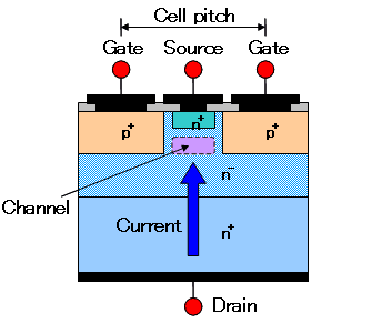
Fig. 3 A schematic diagram of cross-section through a conventional SiC-SIT device
|
|
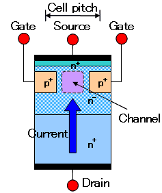
Fig. 4 A schematic diagram of cross-section through a newly developed buried gate SiC-SIT device
|
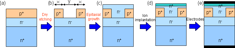
A flow diagram of the manufacturing process for the newly developed buried gate SiC-SIT is shown in Fig. 5. The process consists of five steps as shown below: (a) n
– drift layer and p
+ gate layer are epitaxially grown on n
+ 4H-SiC substrate. (b) The p
+ gate layer is dry-etched to make up a fine groove structure. As the device performance is determined by the accuracy of etching process, i.e. width of p
+ gate area (x) and spacing between two adjacent p
+ gate areas (y), it is a key factor for ensuring high device yield to execute the process with high reproducibility. In the present study, fine groove structure has been fabricated by dry etching after the optimization of etching mask materials, and etching conditions such as gas species, gas pressure, flow rate and exposure time. (c) Over the groove structure, n- channel area is formed by the epitaxial growth, through the optimization of crystal orientation of SiC substrate and growing conditions such as temperature, gas flow rate and so on. (d) n
+ source area is formed by implanting, and activating heat treatment (1600 ºC). Finally, (e) The device is completed by making source, gate and drain electrodes. An cross-sectional scanning electron microscope (SEM) image through an buried gate SiC-SIT prepared in this way shows that the p
+ gate areas are fully embedded n
– channel areas of submicron width are formed between them (Fig. 6).
 |
|
Fig. 5 A flow diagram for the process manufacturing newly developed buried gate SiC-SIT device. The dry-etching technology for making p+ gate area and the epitaxial growth technology over fine groove structures (including pre-processing technology) have been newly developed. |
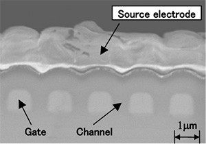
Fig. 6 An cross-sectional scanning electron microscope (SEM) image through a newly developed buried gate SiC-SIT device
|
|
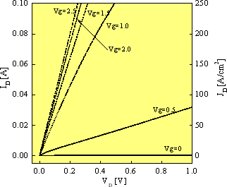
Fig. 7 A voltage-current curve of a newly developed buried gate SiC-SIT device
|
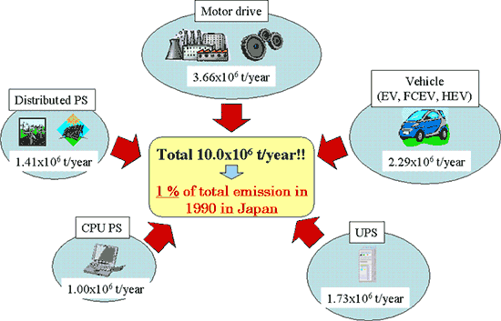
The voltage-current characteristics of newly developed buried gate SiC-SIT shows that RonS at the gate voltage VG = 2.5 V is as low as 1.01 mΩ·cm2 (Fig. 7). In the reverse characteristics, the breakdown voltage VBR is 700 V at VG = -12 V. This RonS is the lowest record among switching devices of 600 V~1.2 kV class breakdown voltage including SiC devices having been announced up to now. In comparison to the performance of Si insulated gate bipolar transistor (Si-IGBT) used for the conventional inverter circuit where breakdown voltage is 600 V and RonS around 12~13 mΩ·cm2, the RonS is reduced to 1/12, and it is expected that the power loss is also extensively reduced to 1/12. If the newly developed buried gate SiC-SIT were put to practical application in various areas, it might be estimated that the carbon dioxide emission in Japan in 2020 would be equivalent to 1 % of the total carbon dioxide emission as of 1990 (Fig. 8).
 |
|
Fig. 8 Estimation of reduction in carbon dioxide emission in Japan in 2020 based on an assumption that the newly developed buried gate SiC-SIT were put to practical use in various areas.(Reference: “Basics and Application of SiC Devices” Published by Ohmsha, Tokyo, in Japanese) |