- Optical Linkage between Electronic Circuits Implemented at Low Cost and Low Voltage -
With the advance of speed and performance of electronic devices in these days, further acceleration in signal transmission between electronic circuits has been demanded intensively. As the conventional signal transmission through copper wiring involves heat production due to resistance, it has been earnestly tried to develop high speed linkage between electronic components through optical means, and a lot of R&D efforts have been paid to low cost production of fast electro-optical (EO) conversion devices in the industrial and academic circles both domestic and overseas.
It has been known that PLZT ceramic materials cause a great change in refractive index when a voltage is applied to sintered ceramic bulk, providing a hopeful prospect for the application to optical linkage technology. When a PLZT film is prepared through the conventional sol-gel process, however, a lot of micro-defects are formed in complicated oxide ceramic structures, to prevent EO function from being derived out of thin film, and to provide serious obstacles for the application to micro-areas such as linkage between electronic circuits.
The AMRI-AIST has been dedicated to the development of ultra-fast EO modulation device meeting the demands for optical linkage (optical interconnection) by using the normal temperature impact solidification based on the aerosol deposition (AD) process developed at the AIST, in collaboration with NEC Corp. under the Nano Structure Forming for Advanced Ceramic Integration Technology Project of the NEDO. Nanotechnology Program. In the AD process, starting materials powder of submicron diameter is blown to a substrate at a high speed under moderate vacuum to form dense ceramic film composed of 10~20nm microcrystals. This method allows creating ceramic film at normal temperatures 300°C or lower at a speed as fast as 1µm/min.
In the present development, it has been successfully achieved to dense and transparent of electro-optical coefficient, as large as 102 pm/V through controlling raw materials composition for the AD process and upgrading the manufacturing process (Fig. 1). The value of EO coefficient is about 6 times as large as that of lithium niobate which is EO film materials having been most frequently used in fast optical modulators so far. The new device will make it possible to reduce the drive voltage for modulation to 1/6 that of the earlier device, and to cut down the length of modulator to 1/6. Down-sizing of the modulator is expected to accelerate the response rate and to implement EO conversion devices working at 100 GHz rate and drive voltage lower than 1V.
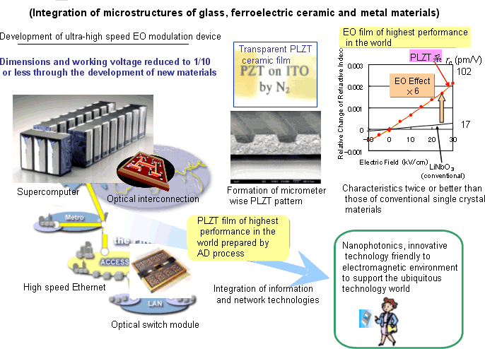 |
Fig. 1. Development of ultra-high speed information processing technology with nano-photonic materials |
*Electro-optical (EO) coefficient is a proportional coefficient of change in refractive index to applied electrical field (=applied voltage/distance). Hence, the unit of EO coefficient is represented by distance (pm, picometer = 1/1012m)/voltage (V). The larger the EO effect is, the lower becomes the applied voltage. As the degree of optical modulation is proportional to the length of optical path and to the change in refractive index, the size of area with refractive index changed is reduced for larger EO effect.
|
References |
-
Nikkei Electronics, September 27, 2004 [in Japanese]
-
Nikkei Sangyo Shinbun, August 24, 2004, and Nikkei Microdevice Web, August 24, 2004 [in Japanese]
-
Nakada, M., Ohashi, K., Lebedev, M. and J. Akedo: Jpn. J. Appl. Phys. 42 (2003), 5960.
-
NEC Press Release (http://www.nec.co.jp/press/ja/0408/2403.html), August 24, 2004. [in Japanese]
-
Jun Akedo: AIST Today, Vol. 8, 4 (2004) [in Japanese]
|