- Integration of Functional Materials and Energy-Saving Ceramics Manufacturing Accelerated -
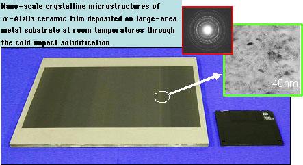
The Advanced Manufacturing Research Institute (AMRI) of the National Institute of Advanced Industrial Science and Technology (AIST), one of independent administrative institutions, succeeded in producing a ceramic film of thickness greater than 1 μm (1 μm = 1/1,000,000 m)with same electrical and mechanical properties as sintered bulk ceramic, in collaboration with Toto, Ltd. (to be designated hereinafter as TOTO). The process consists of spraying α-alumina fine particles of submicron grain size onto a substrate and solidifying it at room temperatures without sintering, through the aerosol deposition method (to be designated as AD method, hereinafter). The AMRI-AIST proved that the ceramic film was formed not by surface melting of sprayed α-alumina particles owing to temperature rises caused by bombardment, but predominantly by modification of fine particles caused through fracture and by surface activation due to new surface formation. The process makes it possible to manufacture ceramic products requiring surface hardness, corrosion resistance and other surface functions without sintering at temperatures higher than 1000 ˚C, as previously needed, leading to extensive energy conservation. TOTO succeeded in providing uniform ceramic coating over a large substrate of area as broad as 200 mm square (Fig. 1), aiming at applications to liquid crystal panels, semiconductor equipment components, electronic circuit board, and so on.
The ceramic film formation based on the solidification of ceramic particles at room temperatures using the AD method was designated as cold impact hardening, and has been applied to manufacture of piezoelectric ceramics such as lead titanate zirconate (PZT) at the AMRC-AIST.
In the joint research with TOTO, where the effects of grain size distribution to mechanical properties were closely analyzed, the process was established for creating ceramic film with mechanical properties such as Vickers hardness, Young’s modulus, dielectric strength, volume resistivity and dielectric constant, comparable to those of sintered bulk, based on cold solidification of α-alumina fine particles. The resultant film had adequate density and nano-scale crystalline microstructures (Fig. 1).
 |
|
Fig. 1. Thick film of α-alumina (Al2O3) formed on metal substrate at room temperatures through the aerosol deposition and its crystalline microstructures.
A ring-like pattern at the top right represents an electron beam diffraction pattern indicating periodic crystalline structure, denying amorphous nature of the ceramic film.
|
The manufacturing process of ceramic materials usually requires sintering at temperatures higher than 1000 ˚C, which makes it difficult to compound or integrate with low-melting point metal. glass or plastics, presenting a serious hindrance for upgrading ceramic electronic components and light-weight construction of structural members. Up to now, a number of research works have been made to reduce the sintering temperatures for the purpose of cutting down energy consumption and implementing innovative functional components through integration with metal or glass materials.
For reducing sintering temperatures to lower than 1000 ˚C, it was attempted to add sintering aids to ceramic raw materials and pulverize raw material powder to nanometer size. But the results were less than adequate: the sintering temperature was lowered only to 900 ˚C. However, electrical, mechanical and chemical properties of ceramic were much inferior to those of ceramic sintered at higher temperatures: lower density, more fragile mechanically, less insulating and more vulnerable to corrosion.
In this study, the AMRC-AIST carried out analysis of film fine structures with a high resolution transmission electron microscopy (HR-TEM), computer simulation of bombardment between fine particles, characterization of film making efficiency, and determination of compressive strength of particles, and demonstrated that fine particles of raw material, α-alumina in submicron size, sprayed on to a substrate were fractured and modified into 10~30 nm-size grains (1 nm = 1/1,000,000,000 m = 10-9 m) to form dense nano-crystalline ceramic film, without surface melting caused by temperature rise (Figs. 1 and 2), and that the activation effects caused by newly created surface at the time of fracture played a central role in binding particles. The experimental evidence for fracture of fine crystal particles is shown in Fig. 2. In this experiment, mixed powder of piezoelectric ceramic material, PZT containing heavy metal such as lead, and _-alumina particles consisting of light elements such as aluminum and oxygen were sprayed onto a substrate to form PZT-alumina complex film at room temperatures. The observation of microstructures under TEM makes it possible to recognize the distribution of two materials as difference in brightness: PZT dark and alumina bright. In a cross-sectional TEM picture shown at the left of Fig. 2, a dark layered area of PZT is seen in parallel to the substrate, i.e., perpendicular to bombardment, corresponding to the size of material particle. Within domains of modified particles, finer crystalline structures of grain size 20 nm or so are observed, as shown in TEM picture of Fig. 1. On the basis of these facts, it may be stated that PZT particles are fractured and modified on clashing to substrate and film surface to form finer crystalline structures, as illustrated in a model at the right of Fig. 2. The resultant ceramic film consists of nano-sized crystalline structures with least amount of amorphous phase at room temperatures. Moreover, it was shown that the cold impact solidification based on the AD process was not restricted to particular ceramic materials, but belonged to phenomena of universal nature, expectedly applicable to non-oxide ceramic materials, such as aluminum nitride for ceramic circuit board, and magnesium diboride for superconducting ceramics.
Following close examination of conditions for suppression of particle aggregation, purity, compressive fracture strength and film formation based on the model shown above, the AMRC-AIST in collaboration with TOTO succeeded in solidifying _-alumina fine particles of 99.9 % purity, which had to be sintered at temperatures higher than 1300 ˚C, at room temperatures without using sintering aids nor organic binder. Properties of resultant ceramic film included: Vickers hardness 1500~2200 Hv, Young’s modulus 300~350 GPa, dielectric strength 150~300 kV/mm or greater, volume resistivity 1.5 x 10¹⁵ &Omega·cm, dielectric constant (ε) 9.8. This is the world’s first achievement of creating ceramic thick film through the cold process having electrical and mechanical properties comparable to those of bulk sintered ceramic. Properties of the latter ceramic include: Vickers hardness 1400~2000 Hv, Young’s modulus 350~380 GPa, dielectric strength 10 kV/mm or greater, volume resistivity 1.5 x 10¹⁵ Ω·cm, dielectric constant (ε) 9.9~10. The newly formed ceramic thick film contained very little pores, and nanometer level smoothness could be obtained through simple polishing. TOTO are making efforts to develop plasma anticorrosive ceramic film, and succeeded in making uniform film of area as large as 200 mm square (Fig. 1).
The present R&D work establishes an epoch making ceramic process, to create ceramic film from low cost α-alumina powder consisting of sub-micron particles without requiring sintering at temperatures higher than 1000 ˚C. The ceramic film produced by this process has same hardness and electrical properties as those of bulk ceramic sintered in conventional manner, and is characterized by high density and smoothness without nanometer-sized pores.
|
|
|
Fig. 2. Microstructures of mixed PZT/alumina ceramic film formed by the aerosol deposition (AD) method and a model of dense film formation based on particle fractures.
|