– Enabling nondestructive inline inspection of drive circuits for displays manufactured with printing methods –
The researchers have greatly improved the sensitivity and inspection area of a thin film transistor (TFT) array inspection technology (a gate modulation imaging technology), and enabled inspection of storage capacitors.
 |
|
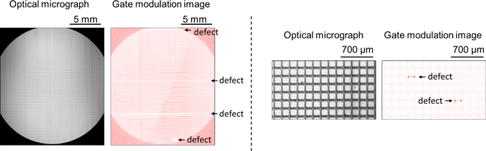
Optical micrograph and gate modulation image measured in TFT defect detection mode (left) and optical micrograph and gate modulation image measured in capacitor defect detection mode (right) |
Development of an all-printing manufacturing technology for displays is an important challenge. However, drive circuits for controlling pixels are composed of a large number of TFTs and storage capacitors, so it is difficult to perform nondestructive inspection in a short time, which inhibits achieving both production efficiency and quality. AIST has developed a unique gate modulation imaging technology that can visualize minute changes in light transmittance and reflectance of TFTs according to gate voltage and inspect drive circuits. In 2014, a 1 mm square could be inspected in about 10 minutes.
In order to increase the sensitivity and inspection area of the gate modulation imaging technology, the researchers combined an image processing unit that can run at a speed of about 1 gigabyte per second, a CMOS camera with about 4.15 megapixels, high-brightness LED lights, and wide view-field optics. This drastically shortened inspection time to within 3 minutes and expanded the area to 3 cm square. At a pixel density of 150 per inch, this corresponds to about 30,000 TFTs. Using changes in optical images of TFT placed in the same pixel as a capacitor with poor insulation, the researchers also made it possible to inspect storage capacitors at once.
The researchers will work on research for commercialization, in order to implement a nondestructive inline inspection technology using this gate modulation imaging technology in printing manufacturing lines for displays and e-paper.