– Promote improvement of next-generation semiconductor device process technology by visualizing defect distribution –
The researchers have developed an image processing technology that can easily detect atomic level defects in a large field of view of a transmission electron microscope image of crystal structures, in collaboration with Toshiba Electronic Devices & Storage Corporation.
 |
|
Schematic diagrams of the technology for visualizing dislocations from transmission electron microscope images |
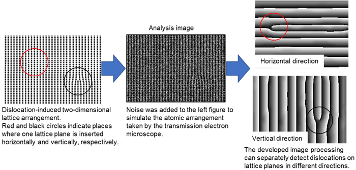
Defect detection is an extremely important issue for quality control of semiconductor devices because a very small defect can lead to output efficiency decline and eventually fatal damage. Atomic level defects are conventionally detected from naked-eye observation of high-resolution images of atomic arrangement taken with a transmission electron microscope. Defect detection in a large area took a great deal of time and effort since the observation field gets narrower with increasing magnification.
The developed defect detection technology applies an image processing technique called the sampling Moiré method. The Moiré fringe pattern can be digitally generated from the atomic array image by treating the atomic arrangement of a crystal as a grid. Simulation study revealed that dislocations could be easily detected from the Moiré fringe pattern because dislocations resulted in discontinuity in the Moiré fringes. As an application, the dislocation distributions in a gallium nitride (GaN) semiconductor were displayed in the Moiré fringe pattern and defect locations were automatically identified.
The developed technique will contribute to improve the treatment process of semiconductor devices by checking the effect of treatment conditions for dislocation reduction, and allow production of high-performance and durable semiconductors.