– Paving the way for possible fabrication of new-generation single-crystal MRAM –
The researchers have developed a stacking technology for a magneto-resistive random access memory (MRAM) to separately form a single-crystal tunnel magneto-resistive (TMR) thin film and then bond it to a CMOS.
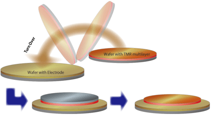
Schematics of 3D process technology
|
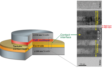
Transmission electron microscope image of a cross-section of MRAM after direct bonding of wafers
|
Until now it was not possible to form a single-crystal TMR device on a polycrystal metal wire. However, this has been made possible by using a 3D stacking process to separately form a single-crystal TMR thin film on a single-crystal silicon wafer and then bond it to a CMOS on another wafer. This technology provides the possibility of using single-crystal materials in the fabrication of MRAM devices. Use of a single-crystal material reduces the variation in its thin film, i.e. the variation among TMR devices to a very low level, when increasing device capacity (miniaturization of TMR devices), and a wide variety of high-performance single-crystal materials can be used.
A non-volatile MRAM consists of a perpendicularly magnetized TMR device as a recording bit, a semiconductor transistor (CMOS) used for bit selection, and metal wires. In the existing fabrication process, the CMOS is formed first, and then metal wires and a polycrystal TMR device are formed and stacked successively on the CMOS to form an MRAM device. In increasing the capacity of MRAM, there were limits on the reduction in variation of the polycrystal TMR device because of atomic-level nonuniformity and unevenness of the device surface, as well as on the choice of materials.
Establishment of the 3D stacking process for the single-crystal TMR thin film and the CMOS wafer will be completed within 2 years.