Update(MM/DD/YYYY):11/09/2016
Demonstration of Stable Operation and Write Error Rate Evaluation of Voltage-driven Non-volatile Memory
- The path to realization of “voltage torque MRAM”, a voltage-driven magnetic memory with ultra-low power consumption -
Points
-
Demonstrated stable operation of “voltage write,” a new write method for non-volatile memory MRAM
-
Developed a method to evaluate a write error rate crucial to practical application, laying the way to realize an error rate necessary for practical use
-
Showed possibility of information equipment loaded with voltage-driven non-volatile memory with ultra-lower power consumption
Summary
Yoichi Shiota (Researcher), Voltage Spintronics Team, the Spintronics Research Center (Director: Shinji Yuasa) of the National Institute of Advanced Industrial Science and Technology (AIST; President: Ryoji Chubachi), demonstrated stable operation of magnetic memory writing using voltage, clarifying the way to realize the write error rate necessary for practical application.
By applying an extremely short voltage pulse for just nanoseconds to a magnetic tunnel junction (MTJ) with a very thin ferromagnetic metal layer (recording layer), it is possible to induce magnetization reversal. Using this technique, information can be written into magnetic memory. AIST demonstrated stable operation with this voltage write, and developed a write error rate evaluation method, evaluating the error rate as 4×10⁻³. Additionally, using computer simulations by which experimental results can be reproduced, AIST showed the possibility of an error rate of 10-10 to 10-15 necessary for memory application by reducing the magnetic damping constant and improving the thermal stability factor Δ or by execution of verification after writing (figure below (b)). The voltage write method does not require a current, so power consumption is extremely low. This achievement is expected to accelerate research and development of the voltage-writing non-volatile memory with ultra-lower power consumption, “voltage torque MRAM.”
Details of the results were published in the preliminary online version of the Japanese scientific journal, Applied Physics Express on December 10, 2015.
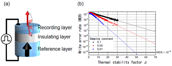 |
(a) Schematic diagram of the newly used magnetic tunnel junction (MTJ) element and (b) thermal stability factor dependence of the write error rate
(a) Applying a very short voltage pulse reverses magnetization (red arrow) of the recording layer.
(b) It is expected that the write error rate will be below 10-15 with a magnetic damping constant of 0.01 and thermal stability factor of at least 50. |
Social Background of Research
Reducing power consumption of IT equipment, the realization of so-called “green IT,” is a critical challenge for realizing a society that is friendly to the environment. One approach to this is the development of non-volatile electronic devices. In the spintronics field, non-volatile memory “MRAM” with zero standby power is being developed using the non-volatile recording function of magnetization. Currently, the electrical current writing system of MRAM (STT-MRAM) undergoing product development globally bears expectations for low power consumption non-volatile memory, but there is a limit to its reduction of power consumption because of power consumption for electrical current writing.
On the other hand, magnetization reversal caused by voltage pulses on the order of nanoseconds has such features as 1) ultra-low power consumption because it does not require a current in principle, 2) high-speed operation on the order of nanoseconds, 3) high write endurance, 4) ability to operate at room temperature. The magnetic memory by voltage writing method, “voltage torque MRAM,” is still at the stage of basic research, but it is expected to become a non-volatile memory with lower power consumption than STT-MRAM in the future.
History of Research
In collaboration with Professor Yoshishige Suzuki of the Graduate School of Engineering Science of Osaka University, AIST has worked to develop technology that controls magnetic anisotropy or the magnetic moment by applying voltage to a metallic magnetic film just a few atomic layers thick (as presented in the May 1st, 2012 AIST press release). Practical application of voltage torque MRAM with this technology requires a write error rate of no more than 10-10 to 10-15. However, so far there has been no example of evaluating the write error rate of the voltage writing method, and it was not known whether there was potential for stable operation as memory.
In this project, AIST worked on evaluation of the write error rate by applying nanosecond voltage pulse to perpendicularly magnetized MTJ which can be used in gigabit-class large capacity memory. In addition, both experimental demonstrations and computer simulations were carried out by AIST towards the realization of write error rates under 10-10 to 10-15.
This research and development was conducted as part of the Cabinet Office “Impulsing Paradigm Change through Disruptive Technologies Program (ImPACT)” research and development program “Achieving Ultimate Eco-friendly IT Equipment Usable Without Charging for Long Periods” (Program Manager: Seiji Sahashi), and received some assistance in the form of research activity start assistance (Issue No.: 26886017), Grants-in-Aid for Scientific Research from the Japan Society for the Promotion of Scientific Research.
Details of Research
A schematic diagram of the voltage writing method is shown in Fig. 1. When not applying voltage, magnetization is oriented in the direction of lower magnetic energy, stable either upward (Fig. 1 left: corresponds to “0” state of memory) or downward (Fig. 1 right: corresponds to “1” state of memory). Applying an ultra-fast voltage pulse here changes the magnetic anisotropy instantaneously and the magnetization of the recording layer begins to rotate (Fig. 1 center). Writing of memory is performed by turning off the voltage exactly when the magnetization turns to the opposite direction of its initial state. The rotation of magnetization is stopped by turning off the voltage and magnetization is fixed to the opposite direction.
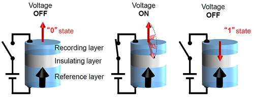 |
Figure 1: Schematic diagram of magnetization reversal by voltage pulse
Magnetization rotates when voltage pulse is applied. Turning off voltage when magnetization is reversed causes magnetic reversal. |
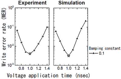
The element used in this research was a cylinder 120 nm in diameter. A 1.8 nm magnetic layer of iron-boron alloy was used as a recording layer, and voltage was applied through an MgO insulating layer. The success or failure of magnetization reversal was determined from changes in the electrical resistance of the element after applying voltage with the write error rate evaluated after each 100,000 write. Figure 2 shows the relationship between the write error rate and voltage application time (time span during which the voltage pulse was applied). A star mark indicates the voltage application time with the lowest write error rate. Because the magnetization reversal technology used this time utilizes rotational motion of magnetization, magnetization reverses effectively when voltage is applied exactly to the time magnetization is half rotated, so the star mark corresponds to that time. The relatively low write error rate of 4×10⁻³ was achieved in experiments. These experiment results are in good agreement with the results of computer simulations assuming a magnetic friction constant of 0.1.
 |
|
Figure 2: The write error rate dependence on voltage application time |
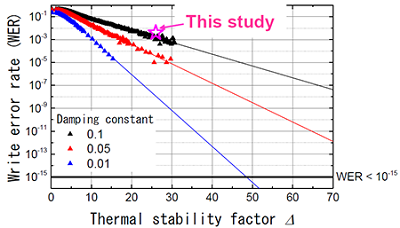
Stable operation of memory becomes possible even at a write error rate of around 10-3, as write error rates of 10-10 to 10-15 necessary for practical use can be achieved if verification is carried out a few times after writing. However, the write speed is decreased by verification. Therefore, write error rates of 10-10 to 10-15 without using verification are necessary to operate memory at ultra-high speed. The results of computer simulations to investigate whether this is possible are shown in Fig. 3. The write error rate (WER) for thermal stability factor Δ was calculated by the computer simulations. The write error rate of 4×10⁻³ was obtained in this demonstration experiment, and this is in good agreement with the simulation result at Δ equal to 26 and magnetic damping constant equal to 0.1. Achieving the write error rate of less than 10-15 might be possible by reducing the magnetic damping constant (to less than 0.01) and improving the thermal stability factor Δ (over 50). MTJ elements with such a magnetic damping constant and thermal stability factor are certainly feasible if a recording layer material with more stable perpendicular magnetization is used and the element size is further miniaturized. In this way, the guidelines for realizing a write error rate necessary for practical application have been obtained. The research and development of voltage torque MRAM with ultra-low power consumption will be accelerated by the guidelines.
 |
|
Figure 3: The write error rate dependence on thermal stability factor Δ |
Future Plans
Based on the guidelines obtained through this research, AIST will develop perpendicular magnetization MTJ elements with low magnetic damping constant and high thermal stability factor Δ, and the precision of voltage writing will be advanced, aiming at realization of a practical application-level write error rate without using verification.