Wataru Mizubayashi (Senior Researcher), Yukinori Morita (Senior Researcher), Hiroyuki Ota (Senior Researcher), Meishoku Masahara (Leader) and others of the Silicon Nano-Device Group, the Nanoelectronics Research Institute (NRI; Director: Tetsuji Yasuda), the National Institute of Advanced Industrial Science and Technology (AIST; President: Ryoji Chubachi), have demonstrated the enhanced performance and high reliability of tunnel transistors (tunnel FETs), which are considered promising technology for future energy-efficient devices.
The researchers developed a process for fabricating both positive and negative-type tunnel FETs, which are indispensable to the CMOS circuit necessary to drive large-scale sensor network circuits, on a cost-advantageous silicon platform, achieved a subthreshold swing value below the physical limits of metal-oxide semiconductor field-effect transistors (MOSFETs), and greatly enhanced the current drivability. The above offers hope that if tunnel FETs are used to drive large-scale sensor network circuits, the long-term reliability, cost advantage, and the ability to make circuits work with a lower-voltage power supply could greatly reduce the cost of establishing and maintaining circuits.
Details of these findings will be presented at the International Electron Devices Meeting (IEDM) to be held on December 15-17, 2014 in San Francisco, USA.
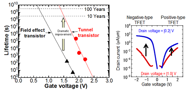 |
Comparison of long-term lifetime of tunnel FETs and MOSFETs (left) and improvement in transfer characteristics of positive and negative-type tunnel FETs (right)
Using the developed process, subthreshold swing value and current drivability are improved. |
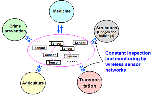
The use of wireless sensor networks that use sensors for constant inspection and monitoring is growing rapidly in a variety of fields, including medicine, crime prevention, agriculture, transportation, and structures (bridges and buildings) (Fig. 1). As Japan’s birthrate falls rapidly and its society ages just as rapidly, such wireless sensor networks are expected to grow larger in the future. Going forward, therefore, sensors will have to conserve energy better and be usable without breaking down over the long term, in order to reduce the replacement cost after installation. Presently, sensors use circuits consisting of MOSFETs, however research in recent years has focused on replacing these with tunnel FETs, which can drive circuits with less power. The key to accomplishing this is whether tunnel FETs can ensure high performance at low voltages, low cost, and long-term lifetime.
 |
|
Figure 1: Diagram of a wireless sensor network |
The Green Nanoelectronics Center (GNC), a collaborative research team (FY2010 - FY2013) within NRI of AIST, researched and developed CMOS devices with a new operating principle designed to cut the power consumption of large-scale integrated circuits (LSIs) by more than 90 %. The devices on which GNC focused its efforts were tunnel FETs, which are highly compatible with conventional CMOS transistors. The outcome of the research was that tunnel FETs gained higher performance as a result of a vertical structure (AIST press release on June 10, 2013) and implementation of an intermediate level in tunnel junctions (AIST press release on June 9, 2014).
This R&D was conducted with financial support from the “Development of Core Technologies for Green Nano electronics” project (Leader: Naoki Yokoyama) of the Japan Society for the Promotion of Science's Funding Program for World-Leading Innovative R&D on Science and Technology (FIRST Program).
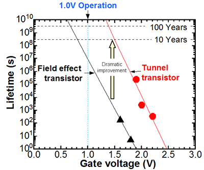
This research first of all verified the long-term reliability of tunnel FETs, with the aim of dramatically reducing replacement costs. Elements used for evaluation were negative-type tunnel FETs, with negative-type MOSFETs used as comparison elements. Long-term lifetime was defined as the time until the threshold voltage shifted 50 mV. If long-term reliability were evaluated under ordinary operating voltage, it would take more than 10 years, which is not realistic. Thus, measured lifetime as found by accelerated testing under higher voltages was extrapolated to the operating voltage to predict lifetime.
Results of long-term lifetime evaluation are shown in Fig. 2. For example, a conventional MOSFET under 1.5 V of gate voltage would last only one thousand and some hundreds of seconds. On the other hand, a tunnel FET would last 10 years, dramatically longer than the MOSFET. This indicates that at drive voltages of 1 V or less, tunnel FETs can provide an operating life of more than a century, allowing them to be used semi-permanently as sensor drive circuits for low-voltage operations.
 |
|
Figure 2: Comparison of long-term lifetime of tunnel transistors and field-effect transistors |
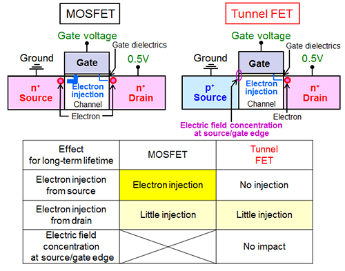
Following is a consideration about the substantial lifetime extensions made possible by tunnel FETs. The long-term lifetime testing shown in Fig. 2 was performed under accelerated testing conditions, with the gates under voltage and with 0.5 V of voltage on the drains on the assumption that they are in operating status. Figure 3 gives an overview of the factors affecting MOSFET and tunnel FET long-term lifetime. The long-term lifetime of MOSFETs is primarily determined by electron injection from the source. In tunnel FETs, on the other hand, the source and drain are of different polarity (positive and negative-types, respectively), and electric fields become particularly concentrated at the positive sources and the gate edges. To date, such electric field concentrations have been suspected of having a harmful effect on reliability. However, this study has shown for the first time that there is hardly any such impact. Additionally, this study also ascertained for the first time that the difference in polarity in tunnel FETs is related to the cause of long-term lifetime. It has been shown that electron injection, which determines the long-term lifetime of tunnel FETs, comes only from negative drains. Because the negative-type drains were under voltage in this accelerated testing, there was little voltage difference between gates and drains, which substantially inhibited the supply of electrons from negative-type drains. This is the reason for the longer lifetime of tunnel FETs.
The above results indicate that if tunnel FETs operating at low voltage were used as sensor drive devices, they could be used semi-permanently without needing to be replaced.
 |
|
Figure 3: Factors affecting MOSFET and tunnel FET long-term reliability |
The study also developed tunnel FET elemental technology aiming at building energy-conserving, large-scale sensor networks.
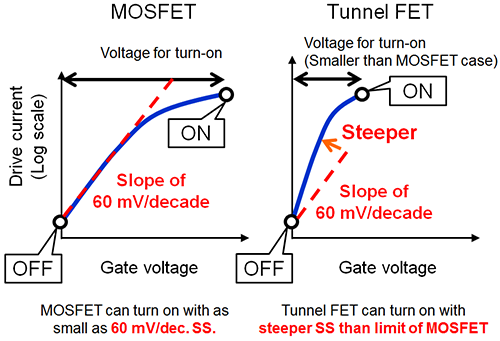
With conventional MOSFETs, carrier injection occurs as a result of thermal diffusion of electrons. Therefore, subthreshold swing, an indicator of a precipitous rise in on/off properties, has a physical lower limit of approximately 60 mV/dec. In tunnel FETs, on the other hand, carrier injection is caused by the tunnel effect, making it theoretically possible to have subthreshold swing values lower than 60 mV/dec. Subthreshold swing is an indicator of at how low a voltage a transistor can be turned on (Fig. 4). Because transistors act as switches in a circuit, the voltage needed to turn a switch on with a tunnel FET is lower than that with a MOSFET. Lowering the voltage of the power supply driving the circuit reduces energy consumption and enables the use of smaller batteries and power supplies.
 |
|
Figure 4: Differences in on/off operation of MOSFETs and tunnel FETs |
Because of these advantages, leading research institutes around the world are striving to develop high-performance tunnel FETs. However, only optimization of single unipolar tunnel FET has been reported so far. CMOS inverters, which are the most basic of circuit elements, require a pair of transistors, a positive and a negative. Because of this, application in actual circuits requires creating tunnel FETs of both polarities on the same platform. In this study, therefore, a new process was developed such that tunnel FETs of both polarities can be made in one pass and circuits can be constructed at low cost (Fig. 5).
It is known that crystal defects at tunnel junctions can cause subthreshold swing to deteriorate. Analysis by X-ray photoelectron spectroscopy showed that cleaning with hydrofluoric acid, which is typically done prior to forming junctions, leaves a very thin oxide layer on the surface, which causes crystal defects. For this reason, the surface was repeatedly oxidized and the oxide layers removed in turn, which eliminated the residual oxide layer and made it possible to form defect-free junctions of tunnel FETs with both polarities. The result was significant improvement in not only subthreshold swing, but also current drivability in both positive and negative-type tunnel FETs. In this study, for the first time, tunnel FETs of both polarities yielded a subthreshold swing value of less than 60 mV/dec., which is the theoretical limit of MOSFETs. The results also showed improved current driviability, approximately 1,000 times greater than announced in the previous press release (Fig. 6). This high performance of tunnel FETs of both polarities is an outcome directly connected to energy conservation with CMOSs, which uses these tunnel FETs as basic structural elements. This technology offers hope of enabling very significant merits, such as applications in circuits capable of driving devices with even tiny amounts of power, such as recovered energy.
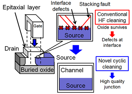
Figure 5: New process for creating tunnel FETs
|
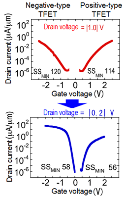
Figure 6: Transfer characteristics of tunnel FETs fabricated with new process
|
The researchers aim to achieve even higher-performance tunnel transistors and use them to replace energy-saving devices for large-scale sensor networks.