Update(MM/DD/YYYY):04/18/2014
Proposal of a New X-ray Non-destructive Inspection Method for Industrial Use
– Previously undetectable defects can now be photographed using X-ray Talbot interferometry –
Points
-
Photographing previously undetectable defects within electronic components using a Talbot interferometer
-
Photographing using a laboratory level small-sized X-ray source that can be easily used on site
-
Expectations for sophistication of and improved efficiency in the quality control of industrial products such as electronic components
Summary
Masato Uehara (Senior Researcher), Process Measurement Team, the Measurement Solution Research Center (Director: Mitsuru Sakamoto) of the National Institute of Advanced Industrial Science and Technology (AIST; President: Ryoji Chubachi), and Atsushi Momose (Professor) and Wataru Yashiro (Associate Professor), the Institute of Multidisciplinary Research for Advanced Materials (Director: Junichi Kawamura) of Tohoku University (President: Susumu Satomi), have demonstrated that internal defects such as voids in the encapsulant of semiconductor packages, which could not be detected by conventional X-ray non-destructive inspection, can be observed using X-ray Talbot interferometry.
X-rays, being able to penetrate through metals, are used for non-destructive inspection of industrial products. However, in addition to metals, industrial products are also composed of materials with a wide variety of X-ray absorption coefficients, including ceramics and resins. It has been difficult to inspect materials such as resins, which have small X-ray absorption coefficients, using conventional X-ray absorption images. On the other hand, with X-ray phase imaging, ample contrast can be obtained even for resins but in many cases, this requires a large synchrotron radiation source, making their use at production sites difficult. With X-ray Talbot interferometry, X-ray phase images can be recorded using a laboratory use X-ray source. Until now, developments of the interferometry have been focused on medical uses. However, AIST proposed its use for the observation of defects in electronic components and conducted experiments. As a result, it has been found that internal defects in resins that could not be observed by conventional X-ray non-destructive inspection can now be observed and this is expected to contribute to the sophistication of quality control.
The details of the results will be published online in Journal of Applied Physics on October 2, 2013 (US EDT).
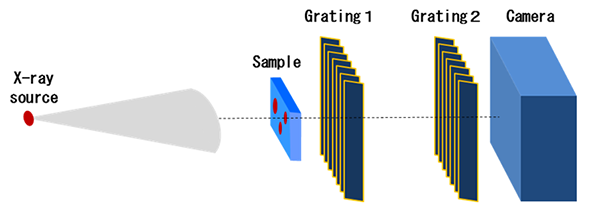 |
(Figure) : Schematic of equipment for X-ray Talbot interferometry
With X-ray Talbot interferometry, a conventional X-ray absorption image, an X-ray differential
phase-contrast image, and an X-ray scattering image can be obtained simultaneously from the moiré image
formed by superpositioning the diffraction images appearing behind grating 1 and grating 2. |
Social Background of Research
To enhance the competitiveness of the manufacturing industry that comprises the backbone of Japanese industry, it is essential to maintain high quality production and high manufacturing efficiency, and accordingly, non-destructive inspection which is directly related to this is a very important technology. This is especially true for electronic components where diverse parts are used and the internal structure is becoming increasingly complicated. Inspection technology which meets these needs is required.
X-ray has been widely used in non-destructive inspection. Using X-ray absorption images which are obtained by conventional inspection, while metal wiring and electrodes within electronic components can be inspected, the encapsulant cannot be inspected. To inspect encapsulants, ultrasound is generally used. However, as this requires immersing the sample in water, it creates difficulties in total inspections.
History of Research
AIST aims to provide production sites with new measuring technologies that contribute to improvements in quality and productivity, measures against product defects, safety, environmental preservation, etc. Hitherto, R&D has advanced the use of X-ray Talbot interferometry in the medical field, but the researchers have made the attempt to photograph electronic components in order to explore the possibility of its application as an industrial use non-destructive inspection method.
The high sensitivity X-ray phase imaging equipment based on X-ray Talbot interferometry used for the present research was developed by Prof. Momose and others of Tohoku University as a part of the Development of Systems and Technology for Advanced Measurement and Analysis Program of the Japan Science and Technology Agency and installed at Tohoku University. The results of this research have been obtained from the use of the high sensitivity X-ray phase imaging equipment installed at Tohoku University under the “Promotion of Use and Dissemination of Research Results” framework of the program.
Details of Research
Figure1 shows the images of an IC package photographed using X-ray Talbot interferometry. An IC package consists of an element, metal wiring, electrodes, and an encapsulant which protects them from external influences. With (a), an X-ray absorption image of conventional non-destructive inspection, while the metal wiring and electrodes can be observed, the structure of the encapsulant cannot be seen at all. On the other hand, with (b), an X-ray differential phase-contrast image obtained by X-ray Talbot interferometry, many voids inside the encapsulant can be observed. These voids are believed to weaken the protection of the encapsulant and pose problems for quality control. X-ray Talbot interferometry provides a more sophisticated non-destructive inspection method.
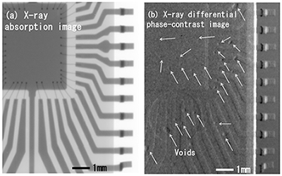 |
Figure 1 : Images of IC Package
(a) X-ray absorption image (conventional non-destructive inspection) and (b) X-ray differential phase-contrast image
While voids in the encapsulant cannot be seen at all in (a), they can be clearly observed in (b). |
Figure 2 shows the images of a simulated sample of power module by X-ray Talbot interferometry. In the simulated sample, an aluminum cooling plate, an insulation plate made of aluminum nitride, and silicon substrate are layered and covered by an encapsulant. Scratches were previously made on the surfaces of the aluminum plate and the encapsulant. These scratches cannot be seen in (a), the X-ray absorption image, but can be clearly confirmed in (b), the X-ray differential phase-contrast image. Furthermore, while the silicon substrate inside the simulated sample cannot be seen at all in either (a) or (b), it can be observed in (c), an X-ray scattering image. A crack made previously in the aluminum nitride plate was not seen in either (a) or (b) but could be clearly seen in (c), the X-ray scattering image.
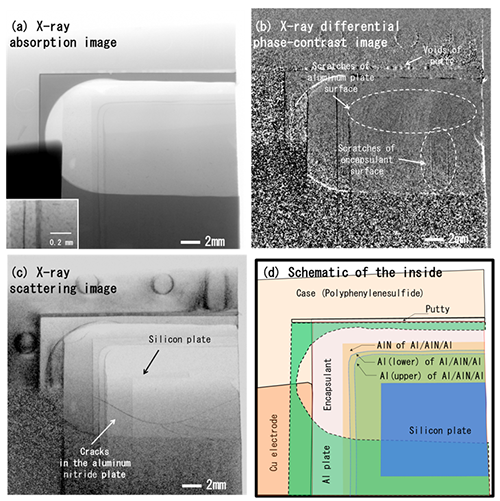 |
Figure 2 : Images of the simulated sample of power module
(a) X-ray absorption image, (b) X-ray differential phase-contrast image, (c) X-ray scattering image, and (d) schematic of the inside
Scratches on the surfaces can be seen in (b) while some cracks in the aluminum nitride plate and
the internal silicon plate can be observed in (c). These cannot be seen in the X-ray absorption
image, which is a conventional X-ray non-destructive inspection method. |
As a result of the photography of electronic components using X-ray Talbot interferometry, it has been shown that voids and scratches on the surfaces in the encapsulant and cracks inside the ceramic insulation plate can be observed in X-ray differential phase-contrast images and X-ray scattering images. These could not be seen at all with conventional non-destructive inspection (X-ray absorption imaging). This is the first time critical defects in an electronic component have been photographed by laboratory level X-ray equipment. X-ray Talbot interferometry makes it possible to obtain an X-ray differential phase-contrast image and an X-ray scattering image simultaneously with a conventional X-ray absorption image, as well as being able to do this with a small X-ray source. This is expected to contribute to the sophistication of X-ray non-destructive inspection equipment for industrial use that can be used on site.
Future Plans
To realize the inspection of thicker products, further X-ray energy enhancements and the manufacture of gratings that can respond to such enhancements will be made. In addition, research will be made into equipment that forms three-dimensional (3D) images like those obtained by the computed tomography (CT), which would allow the location and shape of defects to be grasped in 3D, thus creating equipment which fully meets the needs of production sites.