- It is expected that the efficiency and functionality of CIGS photovoltaic modules will be improved toward mass-production -
Hajime Shibata (Leader), Yukiko Kamikawa (AIST Postdoctoral Researcher), Hironori Komaki (Researcher) and co-workers of the Advanced High Efficiency Processing Team, the Research Center for Photovoltaic Technologies (Director: Shigeru Niki) of the National Institute of Advanced Industrial Science and Technology (AIST; President: Ryoji Chubachi), have achieved for the first time an over 18 % conversion efficiency of a copper-indium-gallium-selenium (CIGS) photovoltaic sub-module (η=18.34, designated area: 3.576 cm2).
CIGS photovoltaic modules and sub-modules generally utilize an integrated structural design that takes advantage of the characteristics of thin-film photovoltaic cells. In a project commissioned by the New Energy and Industrial Technology Development Organization (NEDO), AIST has been engaged in the improvement and optimization of the integration technology in order to reduce the electrical and optical losses that result from the integration process. AIST has also been engaged in an effort to improve the quality of the CIGS light absorption layer. By putting together the formation technology for high quality light absorption layers and the advanced integration technology that had been developed at an earlier stage, the researchers achieved for the first time a high conversion efficiency, over 18 %, of a CIGS photovoltaic sub-module. The developed technology is a core elemental technology for the improvement of the conversion efficiency of photovoltaic modules and is applicable to a wide variety of photovoltaic modules including large-area modules and flexible modules. This technology is expected to contribute to the improvement of the conversion efficiency of mass-produced photovoltaic modules, a reduction in power generation costs, and improvements in the functionality of photovoltaic modules.
 |
|
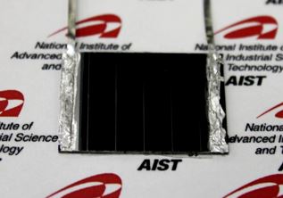
Appearance of the CIGS photovoltaic sub-module that achieved a conversion efficiency of 18.34% (substrate size: 3cm × 2cm) |
CIGS photovoltaic cells are attracting attention as highly efficient photovoltaic cells that can be manufactured at lower cost because a thin light absorption layer of about 2 µm in thickness is enough to absorb sufficient light while inexpensive substrates, including glass and metal thin films, can be used. As shown in Table 1, a conversion efficiency of 14.6 % was achieved recently in a photovoltaic module (125.7 cm × 97.7 cm) from a factory production line. In this way, the conversion efficiency of mass-produced photovoltaic modules is also improving. In general, the conversion efficiency at the module level (the world’s highest: 15.7 %) is lower than the conversion efficiency at the small single cell level (the world’s highest: 20.4 %). Since modules and small single cells differ in many points in terms of the manufacturing method, structural design, etc., the determination of the causes of drops in the conversion efficiency requires complex analysis.
AIST has been engaged in the development of high-quality film formation technology for the light absorption layer of CIGS photovoltaic cells using the multi-source deposition method. Making progress in the optimization of film forming conditions, such as the substrate temperature during the film formation and the material beam flux ratio, AIST established the conditions which made it possible to achieve the world’s highest conversion efficiency level of about 20 % (19.8 % according to in-house measurement) at the small single cell level. In parallel to the above, by conducting research on photovoltaic sub-modules, which are intermediate configuration between single cells and modules, AIST has been trying to identify and address the causes of the falls in the conversion efficiency that are inherent to the integration process. Improving the integration processes of laser scribing and mechanical scribing employed in the present work, which are basically the same processes used in the manufacture of commercial modules, AIST reduced the adverse impact of the integration process on the product characteristics, and achieved in 2011 the world’s highest conversion efficiency level of 16.6 % in a photovoltaic sub-module fabricated on a glass substrate. AIST has also been engaged in the development of technology for fabricating photovoltaic modules on flexible substrates and achieved in February 2010 a conversion efficiency of 15.9 % with a flexible photovoltaic sub-module having an integrated structural design (AIST press release on February 25, 2010). This time, with further advancement and improvement of the integrated structural design, AIST put together the integration technology and the formation technology for high-quality CIGS light absorption layers.
This R&D project was carried out as a part of a project, "The Development of Next-Generation High-Performance Technologies for Photovoltaic Systems (FY2010-2014)", commissioned by NEDO.
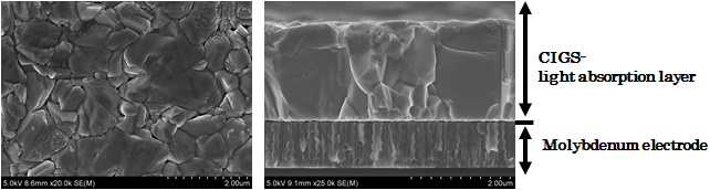
A CIGS photovoltaic sub-module was produced using a soda lime glass substrate, a type of substrate commonly used for CIGS photovoltaic cells. The advanced CIGS film formation technology achieved by earlier research was used to produce a uniform, high-quality light absorption layer that had excellent surface flatness due to the scarcity of microscopic dimples (voids) on the surface (Fig. 1).
 |
|
Figure 1 : SEM images of the CIGS light absorption layer surface (left) and a cross-section of the CIGS light absorption layer and molybdenum electrode (right) |
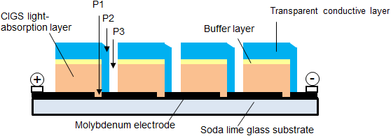
Figure 2 outlines the cross-section of the fabricated photovoltaic sub-module. An integrated structural design connecting four photovoltaic cells in series was used. The integrated structure is formed as a result of the following processes: separating the molybdenum (Mo) electrode by means of laser scribing (P1), separating the buffer layer and the CIGS light absorption layer by means of mechanical scribing (P2) and separating the transparent conductive layer, the buffer layer, and the CIGS light absorption layer by means of mechanical scribing (P3).
 |
|
Figure 2 : An outline of the cross-section of the fabricated photovoltaic sub-module |
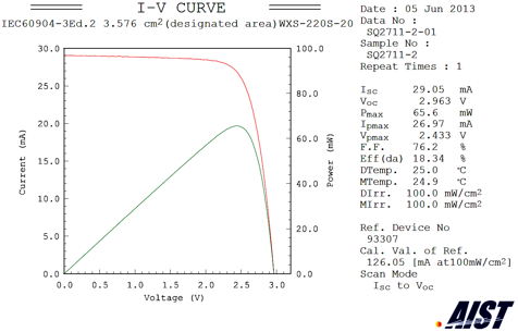
These scribed areas are "dead" areas that do not generate photocurrent in the photovoltaic cells and thus they cause a loss of photocurrent. The researchers minimized the electrical losses from the integration process by optimizing scribing conditions, geometrical patterns, etc. They also reduced the optical losses by decreasing the size of the "dead" areas. As a consequence of having put together the advanced integration technology and the formation technology for high-quality CIGS light absorption layers, the researchers achieved for the first time a conversion efficiency of over 18% at the sub-module level (η=18.34 %, open-circuit voltage: 2.963V, short-circuit photocurrent: 29.05 mA, fill factor: 76.2 %, designated area: 3.576 cm2) (Fig. 3).
The advanced integration technology and the formation technology for high-quality light absorption layers established in the present study are expected to be applied to a wide variety of photovoltaic modules including large-area modules and flexible modules.
 |
|
Figure 3 : The power generation characteristics of the fabricated CIGS photovoltaic sub-module
The figure shows official data, prepared by an independent organization that evaluated the conversion efficiency of the fabricated sub-module. The red line in the graph represents the current-voltage curve while the green line represents the output-voltage curve. The peak in the green curve indicates the maximum output. Eff(da) is the conversion efficiency; VOC the open-circuit voltage; F.F. the fill factor; ISC the short-circuit current. |
The researchers plan to apply the developed elemental technology for the manufacture of CIGS photovoltaic modules to the manufacture of larger sub-modules and flexible sub-modules, and improve the efficiency and functionality of CIGS photovoltaic sub-modules.