Naoki Yokoyama (Leader), Shintaro Sato (Specified Concentrated Research Specialist), Daiyu Kondo (Specified Concentrated Research Specialist) and co-workers of Collaborative Research Team Green Nanoelectronics Center (GNC), the Nanoelectronics Research Institute (Director: Seigo Kanemaru) of the National Institute of Advanced Industrial Science and Technology (AIST: President: Ryoji Chubachi), have developed a low-resistivity and highly reliable interconnect using multi-layer graphene, which is a two-dimensional nanocarbon material.
In conventional technology, graphene is obtained mainly through the exfoliation of graphite crystals, whereas this new technique synthesizes multi-layer graphene on a substrate by the chemical vapor deposition (CVD) method using a cobalt epitaxial film as a catalyst. This multi-layer graphene has a structure and electrical properties similar to those of graphene obtained from high-quality, crystalline graphite. In addition, it is more tolerant than copper to high current densities. Furthermore, by intercalating different molecules (iron chloride) between the layers of the multi-layer graphene, the researchers achieved the same order of resistivity (9.1 µΩ cm) as that of copper. The resistivity is about one order of magnitude smaller than that of graphene synthesized using the conventional CVD method. The newly developed interconnect is expected to be applied to the interconnect of large-scale integrated circuits (LSIs) to reduce energy consumption.
The details of this technique will be presented at the International Interconnect Technology Conference (IITC 2013) to be held from June 13 to 15, 2013, in Kyoto.
 |
|
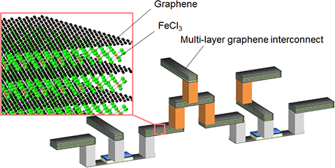
Schematic diagram of LSI using multi-layer graphene interconnects |
In recent years, with the popularization of mobile information devices and the increased functionalization of IT equipment, increased electrical power consumption has become a concern, and reducing this consumption has been desired. Conventionally, LSIs have been designed to reduce power consumption through miniaturization; however, the miniaturization is approaching its limits and various adverse effects have been pointed out. Copper is used for the interconnect of leading-edge LSIs. As the interconnect becomes narrower, the electrical current density increases, the tolerance to electromigration decreases, and thus reliability is reduced. Furthermore, miniaturization causes the increase in the effective resistivity due to the scattering of electrons at crystal grain boundaries and on surfaces and the barrier metals that cannot be thinned beyond a certain point. There is therefore a need for a new interconnect material that replaces copper.
Graphene can sustain an electrical current density two orders of magnitude higher than that of copper, and graphene could have low resistivity because it shows ballistic conduction. It is therefore expected to be used as a wiring material for miniaturized LSIs. However, technology for the large-area synthesis of high-quality multi-layer graphene suitable for interconnects has not yet been established. In addition, multi-layer graphene interconnects with the same resistivity as copper have never been realized.
GNC was established in April 2010 to implement a project selected for FIRST, which is managed by the Cabinet Office, Government of Japan, and the Japan Society for the Promotion of Science. The members of GNC are researchers from five companies (Fujitsu Ltd., Toshiba Corporation, Hitachi Ltd., Renesas Electronics Corporation, and ULVAC Inc.) and AIST researchers.
With the goal of reducing power consumption of LSIs to 1/10 to 1/100 of that of conventional ones, GNC has been studying how to apply graphene and carbon nanotubes to interconnects and transistors since 2011. This research and development project was supported by the FIRST project “Development of Core Technologies for Green Nanoelectronics” (Lead Researcher: Naoki Yokoyama).
The researchers have developed a technology for synthesizing high-quality multi-layer graphene. At the same time, by intercalating different molecules they have succeeded in using the graphene to make an interconnect with a low resistivity of the same order as that of copper interconnects. The new technology is described below.
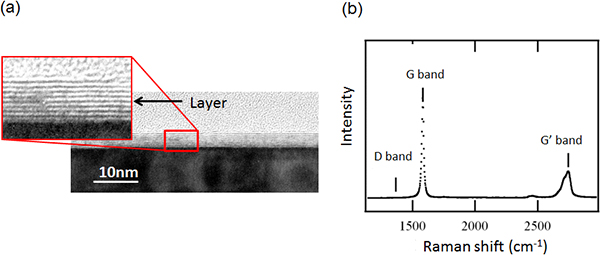
The developed technology synthesizes high-quality multi-layer graphene on a sapphire substrate by the thermal CVD method under an optimized condition. The source gas is methane diluted with argon and hydrogen, and the catalyst is a thin film of cobalt formed using the sputtering method on the sapphire substrate, which is heated to about 500 ℃. The graphene synthesis temperature is about 1000 ℃. Figure 1 shows transmission electron microscope (TEM) images of the cross section of the synthesized multi-layer graphene, and its Raman spectrum. The TEM images indicate that the multi-layer graphene has about 10 layers. Because the shape of the G’(2D) band in the Raman spectrum is similar to that of high-quality, crystalline graphite, it is possible that this multi-layer graphene has a structure similar to that of graphite.
 |
|
Figure 1 : (a) Cross-sectional TEM images and (b) Raman spectrum of multi-layer graphene |
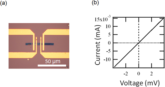
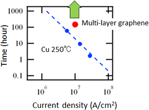
The newly developed multi-layer graphene was transferred onto a silicon substrate with an oxide film and an interconnect was made using typical semiconductor processes. Figure 2 shows an optical microscope image and current–voltage characteristics of the graphene interconnect. The minimum resistivity was 56 µΩ cm, which was comparable to that of high-quality, crystalline graphite (resistivity about 40 µΩ cm). A current of 107 A/cm2 density was applied to the graphene interconnect at 250 ℃. The interconnect was still not broken after 150 h, and it had better tolerance to high current density than did copper wiring (Fig. 3).
 |
|
Figure 2 : (a) Optical microscope image and (b) current–voltage characteristics of multi-layer graphene |
 |
|
Figure 3 : Evaluation of current density tolerance at 250 ℃
Blue dots indicate the conditions under which copper interconnects broke. The multi-layer graphene interconnect did not break, even after the application of 107 A/cm2 current for 150 h. |
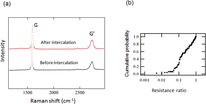
Despite the excellent reliability of the developed multi-layer graphene interconnect, its resistivity was more than one order of magnitude higher than that of copper. The researchers therefore attempted to lower the resistivity by intercalating iron chloride. The intercalation was done by placing a multi-layer graphene interconnect formed on a substrate and iron chloride powder into a quartz tube under vacuum and heating it to 310 ℃. Figure 4 shows the Raman spectra before and after the intercalation and the rate of change in resistivity. The G band in the Raman spectra shifted to the higher wavenumber region, suggesting that charges are transferred to the multi-layer graphene as a result of the intercalation. Such charge transfer should lower the resistivity, and in fact the resistivity of the multi-layer graphene decreased by a median of 15% after the intercalation. The minimum resistivity value obtained was 9.1 µΩ cm. For the first time, the same order of resistivity as that of copper was achieved in multi-layer graphene interconnects.
 |
|
Figure 4 : (a) Raman spectra before and after intercalation. The G Band shifted to the higher wavenumber region. (b) Cumulative probability distribution of rate of change in resistivity after intercalation. The median rate was 15%. |
The developed multi-layer graphene interconnect with low resistivity and high reliability is expected to be used as LSI interconnects. The researchers aim to realize a multi-layer graphene interconnect that has lower resistivity than copper. At the same time, they will attempt to develop three-dimensional wiring using multi-layer graphene and carbon nanotubes for application to LSIs.