Update(MM/DD/YYYY):02/07/2013
Theoretical Prediction of Enhanced Resolution of Helium Ion Microscope Images
- This study contributes to the development of nano-scale devices using graphene -
Points
-
A first-principles calculation method that predicts images taken by a helium ion microscope (HIM)
-
The calculations suggest enhancement in HIM resolution that enables us to take lattice image of graphene.
-
Higher resolution observation of nano-scale device can accelerate research and development of them.
Summary
Yoshiyuki Miyamoto (Leader), Dynamic Process Simulation Group, the Nanosystem Research Institute (Director: Tomohiko Yamaguchi) of the National Institute of Advanced Industrial Science and Technology (AIST; President: Tamotsu Nomakuchi), has developed a computational method to predict images taken by a helium ion microscope (HIM) and applied this prediction method to the images of graphene which is an important material for developing nano-scaled devices, in collaboration with Prof. Hong Zhang, Sichuan University, China, and Prof. Angel Rubio, the University of País Vasco, Spain. The calculations clarified the necessary resolution of HIM to obtain the lattice image of graphene.
HIM can perform non-destructive imaging of materials with a low dose of the helium ion beam, while can process materials with a higher dose of the beam. The present research applied a computational scheme to HIM and showed the possibility of further enhancement in resolution of HIM images near future. This result would contribute to the development of materials indispensable for nano-devices.
The detail of this research will be published in Physical Review Letters published by American Physical Society on December 28, 2012.
 |
|
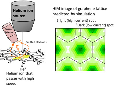
(Left) Scematic of HIM, (Right) HIM image of graphene lattice predicted by simulation |
Social Background of Research
HIM takes images by detecting electrons which were emitted by the collision of helium ions. Similar to a scanning electron microscope (SEM), HIM can perform non-destructive imaging of samples as fabricated in a device structure, and take higher-quality images compared to those measured by SEM. However, the principle of HIM imaging as well as the limit of resolution was unknown. Thus, theoretical studies on the principle of HIM imaging have been awaited.
History of Research
AIST introduced HIM and applied it to the measurement and fabrication of graphene devices. (AIST press releases on September 25 and December 11, 2012) Meanwhile, AIST has been conducting the development of a computational simulation technology for real-time electron dynamics aiming at the establishment of simulation technologies for designing structures, production, and characterization of materials based on the quantum mechanics using the first-principles calculations. In the present research, the computational technology for electron dynamics was applied to HIM imaging which has attracted attention as a technology for material/device characterization. AIST performed the numerical calculations by using the Earth Simulator.
This research was carried out as a part of an Earth Simulator Proposed Research Project, "Large-scale Simulation on the Properties of Carbon-nanotube" (Project Representative; Satoshi Nakamura, Research Organization for Information Science and Technology), of the Earth Simulator Center, Japan Agency for Marine-Earth Science and Technology.
Details of Research
In this research, a computational technique which follows real-time electron dynamics based on the time-dependent density functional theory was used to compute the amount of electron emission by irradiating one graphene layer with a helium ion beam of kinetic energy of 30 keV. The calculations were made on six ion beam-irradiation points, A-F, shown in Fig. 1.
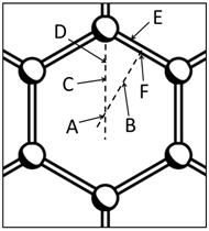 |
Figure 1 : Irradiation points of helium ion beam (A-F) assumed in the present simulations
Open circles denote carbon atom positions of graphene. |
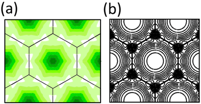
According to the first-principles simulations, the amount of emitted electron increased in the order A to F (helium irradiation points) shown in Fig. 1. Figure 2(a) shows the simulated HIM image of graphene which was obtained by interpolating the calculated amounts of emitted electrons depending on irradiation points. Figure 2(b) shows graphene electron density distribution, which shows strong correlation with the simulated HIM image.
 |
|
Figure 2 : (a) Simulated HIM image of graphene (b) Electron density distribution of graphene |
Assuming that a simulated HIM image is similar to electron density distribution, material structures can be analyzed using already obtained HIM images by experiments. Figure 2 is a simulated result assuming the diameter of helium ion beam as that of helium nuclei, namely the size-less point. On the other hand, the radius of currently available helium ion beam corresponds to the triple of the effective helium atomic radius, which can be included in simulated HIM images by introducing "broadening" in the electron density profile shown in Fig. 2 (b).
Figure 3 shows HIM images approximated from the electron density distribution at an edge of graphene ribbon. Gaussian-broadening (Δr) that corresponds to the half of diameter of helium ion beam was applied to the electron density distribution to approximate the HIM images. The left image was obtained by assuming an ultra-thin diameter of helium ion beam corresponding to the helium nuclei, which shows atomic resolution. The right image was approximated by assuming the diameter of currently available helium ion beam, which shows uniform electron emission at the central part of graphene ribbon while shows a flat image at the edge with gradually decreasing electron emission. Meanwhile, the central image was simulated by assuming a slightly narrower diameter of helium ion beam, which can shows a honeycomb lattice image of graphene even though it cannot reach to the atomic resolution. This result suggests that the graphene lattice would be observed with a diameter of helium ion beam smaller than that of currently available beam.
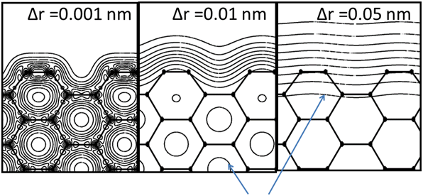 |
Figure 3 : Simulated HIM images with different diameters of helium ion beam (about four times of Δr)
The blue arrows indicate the contour lines of maximum electron emission. |
The mechanisms of electron emission upon collision of helium ion to the sample was thought as processes accompanying to the neutralization of the helium ion or processes that accompanies to core-electron excitation in carbon atoms. However, the present simulation revealed the low neutralization probability of the helium ion that go through graphene because its velocity is too fast. Experimentally measured and reported kinetic energy of the emitted electron is in the order of few eV that is too low to excite carbon atom's core electrons. Therefore, the mechanisms mentioned above are unlikely. The present computational results suggest that the impact ionization of a helium ion causes secondary electron emission.
Future Plans
With use of the computational method, the researcher will contribute to the development of device technology through the characterization of the quality of nano-device materials using HIM.