Tatsuo Hasegawa (Deputy Director), the Flexible Electronics Research Center (FLEC; Director: Toshihide Kamata) of the National Institute of Advanced Industrial Science and Technology (AIST; President: Tamotsu Nomakuchi), Toshikazu Yamada (Senior Researcher), Flexible Organic Semiconductor Team, and others of FLEC, and the Electronics and Photonics Research Institute (Director: Satoshi Haraichi) of AIST, have developed a manufacturing technology for highly uniform thin films of organic polymer semiconductors without material losses by applying the semiconductor solution on a highly hydrophobic surface that strongly repels the solution. The technology allows remarkably simple production of high performance thin-film transistors (TFTs) that are indispensable building blocks for information terminal devices such as electronic papers.
It is known that conventional solution (or wet) processes for thin-film production is not compatible with highly liquid-repellent (or hydrophobic) surfaces, although the employment of such surfaces as the gate dielectric surfaces is quite effective in improving the stability of TFT characteristics. In this study, the researchers developed a new "push coating" technique to produce organic polymer semiconductor films on highly hydrophobic surfaces, where a solution of organic polymer semiconductor is compressed with an original silicone-rubber-based trilayer stamp to wet the hydrophobic surfaces uniformly by way of the capillarity. The technique allows the production of uniform and highly crystalline semiconductor thin films on hydrophobic surfaces. It causes almost no material loss, in striking contrast to any other solution processes. Improved crystallinity of the films was confirmed using the synchrotron radiation facilities at the High Energy Accelerator Research Organization (KEK; Director General: Atsuto Suzuki). It is expected that the developed technology would greatly accelerate the research and development of flexible electronic devices, and also that the technology should be applicable to thin-film processing of a wide range of materials.
The details of this study will be published online in a British scientific journal, Nature Communications (doi:10.1038/ncomms2190).
 |
|
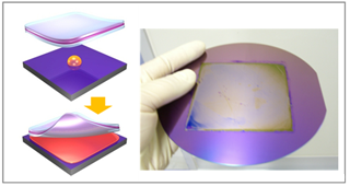
Schematic of the push coating technique (left) and the obtained polymer semiconductor film (right) |
The solution processes that are used to manufacture thin films by applying material solutions on substrate surfaces are widely utilized as convenient film production techniques where vacuum conditions are not necessary. Particularly, the "printed electronics" technology which is a technology for fabricating electronic devices by forming metal and semiconductor films using the techniques and their evolved form, "printing", attracts considerable attentions in recent years. It is expected that the printed electronics technology should enable the production of large-area electronic devices, such as electronic papers and sensor sheets, without the use of huge vacuum facilities and the easy adoption of roll-to-roll processes by using flexible sheets, so that the technology should revolutionize the future electronics industry.
In order to employ the solution processes for the semiconductor thin film production, a primarily requirement is to wet substrate surfaces uniformly with the semiconductor solution. On the other hand, TFT device characteristics become considerably stabilized by the use of gate dielectric layers whose surfaces strongly repel the solution. As a result, conventional solution techniques suffer from a serious problem; it is quite difficult to achieve uniform films or to avoid considerable loss of the raw materials, as the highly hydrophobic surfaces repel the solutions. Therefore, the main challenge in the field of printed electronics is to find out a way to wet highly hydrophobic surfaces uniformly, although the subject apparently includes a contradiction.
AIST has been promoting the research and development of the printed electronics technology in a wide range of aspects. A part of the research and development has focused on a novel solution process which is available to produce the films of organic polymer semiconductors, which are suitable for solution processes, on highly hydrophobic surfaces. Spin coating that is a representative solution process is highly material-consuming especially on highly hydrophobic surfaces, where most of the material should be lost. It is also difficult in drop-cast or the relevant techniques to wet highly hydrophobic surfaces and produce large-area and uniform semiconductor thin films. The researchers have been conducting the development of a novel push coating technique, where the conformal contact between a dielectric layer surface and the original stamp composed of three silicone-rubber-based layers with different properties; the technique enables uniform wetting of the highly hydrophobic dielectric surfaces with a small amount of the solution. This study is supported by the Japan Science and Technology Agency through Strategic Promotion of Innovative Research and Development Program (S-Innovation), as “Development of Flexible Display based on AM-TFTs Manufactured by Printing Processes with New High-Performance Polymer Semiconductors ” (FY 2009 - ), and also partly by the Japan Society for the Promotion of Science through the Funding Program for World-Leading Innovative R&D on Science and Technology (FIRST Program), as “Quantum Science on Strong Correlation” (FY 2009 - 2013).
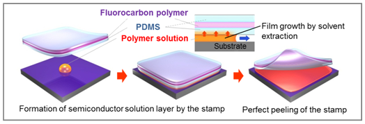
Figure 1 shows a schematic of the push coating technique for the thin-film production. The researchers designed and fabricated a PDMS/fluorocarbon polymer/PDMS trilayer stamp in which the PDMS layers work as surface-contact layers on both sides and the fluorocarbon polymer works as a blocking layer against solution penetration. The stamp has superior flat surface (root-mean-square roughness of 1.20-1.36 nm), absorbs solvent slowly, and retains it within the surface-contact PDMS layer, while the stamp deformation is minimized against solvent sorption. The film production process is composed of the following three steps: 1) formation of a thin semiconductor solution layer by compressing a solution droplet by the stamp, 2) film growth induced by solvent absorption and retention in the stamp, and 3) peeling off the stamp and formation of a whole semiconductor polymer film on the substrate.
 |
|
(Figure 1) : Schematic of the film production process by the push coating technique |
Figure 2 presents an example for the obtained films; a film of a typical polymer semiconductor (P3HT, poly(3-hexylthiophene)) is fabricated on a silicon wafer with a silicon dioxide layer (300 nm in thickness) whose surface is modified by a silane-coupling agent to have highly hydrophobic characteristics (water contact angle of 110 °). The films with thickness of 50 nm and area of 10 cm square were obtained from 350 µL of 0.1 wt% solution of the polymer semiconductor in 1,2,4-trichlorobenzene.
 |
(Figure 2) : P3HT film produced by the push coating technique on highly hydrophobic surface
Upper right : Water contact angle on the substrate surface |
The advantages of the push coating technique are a wide range of controllability in terms of film processing conditions (temperature, duration, and kinds of solvents), and a facile and perfect peeling capability of the stamp from the semiconductor polymer films even after a very long stamping duration for the film growth or from the films on highly hydrophobic surfaces (with small surface energy). Note that the use of the newly designed trilayer-structured stamp enables these advantages. It takes several minutes for the stamp to absorb the solvent, and the solvent retention in the stamp lasts during the film growth. Since the stamp surface is kept semi-wet for a long period of time, the adhesion force at the stamp-film interface is weaker at any time than that at the film-substrate interface. This feature allows a whole film left on the substrate surface after a long stamping duration. The stamp can be cured by solvent desorption and is reusable for more than 10 times.
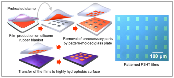
Because the films can in principle be manufactured on any flat surfaces by the push coating technique, a variety of fine patterning processes can be used after the film formation. An example of a simple fine pattering process using the push coating is illustrated in Fig. 3. A semiconductor polymer film was first fabricated on top of a plane silicone rubber blanket by the push coating technique, and then unnecessary parts of the film were removed to obtain patterned films by the reverse printing technique. Finally, the patterned films were transferred from the blanket to a highly hydrophobic gate dielectric surface. A fairly fine patterning with 200 ppi resolution was realized in the process.
 |
|
(Figure 3) : Negative image patterning process for a push-coated film |
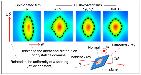
As the push coating technique has remarkable controllability of film forming conditions, it enables the improvement in the crystallinity of semiconductor polymer films. For evaluating the thin-film crystallinity, the researchers conducted synchrotron-radiated x-ray diffraction measurements at Photon Factory, the synchrotron radiation facilities of KEK. Figure 4 presents contour color maps of x-ray diffractions (half maxima are shown by dashed curves) for polymer films processed at various temperatures. It was found that the width along the 2θ direction decreased as the processing temperature increased. The result indicates that the higher processing temperature allows the film growth with a higher order of molecular arrangement (or thin-film crystallinity). From the analyses of diffraction peak profiles, it was shown that the push-coated films processed at high temperature are composed of crystalline grains with uniform d spacing (~ 1.64 nm), while the spin-coated films fabricated at room temperature are composed of grains with distributed d spacing (1.64–1.69 nm). It was concluded that the push coating technique has advantages in producing thin films with higher uniformity and crystallinity by optimizing the processing conditions.
 |
|
(Figure 4) : Peak profiles of the x-ray diffractions for the films processed at different conditions |
Bottom-gate, bottom-contact P3HT TFTs were fabricated using these semiconductor polymer films. The maximum carrier mobility of the TFTs using push-coated films reaches 0.47 cm2/Vs, which is about 10 times higher than those of TFTs using spin-coated films.
In contrast to the spin coating technique, the push coating technique has the following unique advantages;
-
Applicable to any substrate-solvent combination, including high boiling point solvent and highly hydrophobic substrate. No additional surfactant is necessary to control the surface wettability.
-
Film production with minimized amount of solution is possible. Almost all semiconductor material in solution is utilized to form films as the loss of the material due to the repulsion of the solution can be avoided.
-
Processing time, temperature, film thickness, and coating area can be set freely.
From these advantages, a wide range of application of the technique as a versatile technique for thin-film processing is expected.
The researchers will further optimize the printing conditions, semiconductor materials, and device structures, and improve the performance and stability of TFTs. They also plan to manufacture high-performance active backplanes using whole printing processes, by combining the various printing techniques for metal wires, electrodes, etc.