- Evolution toward next-generation IC boards and micro printed circuit boards for cell phones and IC tags -
SIJ Technology, Inc., IOX Co., Ltd, NGK Spark Plug Co., Ltd., Osaka Municipal Technical Research Institute (OMTRI), and the National Institute of Advanced Industrial Science and Technology (AIST) have jointly realized ultra-fine wires with a line width of 5 µm and specific resistivity of 8.1 µΩ·cm through the research commissioned by the New Energy and Industrial Technology Development Organization (NEDO). The wires were fabricated by direct patterning with an inkjet technology and a technology for reduction under extremely-low oxygen partial pressure. The wires are expected to contribute to the development of next-generation IC boards and micro printed circuit boards for cell phones and IC tags.
The main purpose of this research is to integrate the elemental technologies—the nanoparticle production technology, the technology for reduction under extremely-low oxygen partial pressure, and the ultra-fine inkjet technology—to develop an ultra-fine copper wiring technology for next-generation IC boards. Further downsizing and microminiaturization are required for the IC boards and this is the technological driving force for such ultra-fine wiring. Accordingly, the following goals have been set:
-
High migration resistance using copper wires
-
Improving the wire conductivity by using the technology for reduction under extremely-low oxygen partial pressure
-
Using nanoparticles for fabricating ultra-fine wires with a line width of 5 µm or less
-
Achieving cost reduction through process simplification by using direct inkjet patterning
In recent years, the densification of various electronic parts has become imperative for downsizing electronic devices and realizing high functionality. Generally, metal wires with a line width less than 10 µm are formed by first depositing a metal film by sputtering or vapor deposition in a vacuum and then using lithography and etching techniques. However, the process requires a large sputtering system and an exposure system, both of which are costly, and it is necessary to remove a part of the deposited metal film that is not used for wiring. Therefore, a printable electronics technology is desired that can realize fine wires with a line width of 20 µm or less in an eco-friendly manner without using wet processes such as etching and can reduce the cost of electronic devices.
In another aspect, gold and silver are generally used as metal nanoparticles in the ink used for fabricating fine wires, and methods have been established to form fine wire patterns with them. However, gold is an expensive material, and this causes cost issues and prevents the wide use of gold nanoparticles. Silver nanoparticles are much less expensive, but in reducing the line width and space, an inherent problem looms large—migration, which causes short-circuit failures. Therefore, establishing a technology to produce copper-nanoparticle ink, replacing silver with copper is attracting attention.
Downsizing and microminiaturization in IC packages are particularly important among the requirements for electronic parts (Fig. 1). The role of an IC package is to protect the IC chip from the external environment and to electrically connect the motherboard and the IC chip; IC packages contain wires for the latter purpose. The wires in IC packages are becoming narrower and narrower so that a wire pitch of 10 µm or less is expected to become the global standard by about 2018 (Fig. 2). To meet the above-mentioned requirements, in 2010, the research group started a project to integrate the elemental technologies: the nanoparticle production technology, the technology for reduction under extremely-low oxygen partial pressure, and the ultra-fine inkjet technology.
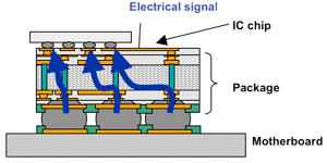
Figure 1: IC package
|
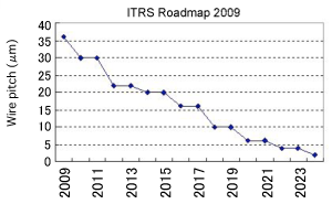
Figure 2 : Wiring rules for IC packages
|
In general, application development of an inkjet technology by a single company is difficult, and cooperation among three types of enterprises—one with an ink technology, another with an inkjet technology, and the last with a board technology—is required. The present R&D is based on the technology for reduction under extremely-low oxygen partial pressure and the ultra-fine inkjet technology of AIST. IOX Co., Ltd. and Nanomaterials Laboratory, Organic Materials Research Division, OMTRI, have developed conductive ink using copper nanoparticles. SIJ Technology, Inc. has developed an ultra-fine copper wiring process. NGK Spark Plug Co., Ltd. has performed the evaluation of those developments for practical applications. The R&D system is a joint effort involving the combination of upstream industries with elemental technologies and a downstream industry performing evaluation toward practical use. In this system, problems related to materials and apparatuses are clarified and addressed so that the development of the elemental technologies is accelerated. The present R&D has been performed jointly as a commissioned project under Research and Development of Nanodevices for Practical Utilization of Nanotechnology of NEDO, and the result presented here was obtained through the project.
With wide knowledge and the technical strength required for the fabrication of nanoparticles, IOX Co., Ltd. and OMTRI have jointly developed copper nanoparticle ink for inkjet printing.
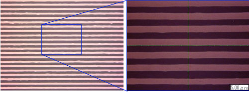
Using the copper nanoparticle ink and ultra-fine inkjet technology, SIJ Technology, Inc. succeeded in forming lines with a width of 5 µm and a pitch of 10 µm on glass substrates based on the evaluation of inkjet compatibility and the optimization of ink discharge conditions (Fig. 3).
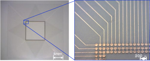
In addition, to showcase a more realistic application, wires were formed on an epoxy board to mimic a package board for high-end ICs. NGK Spark Plug Co., Ltd. designed the wire pattern with a minimum line width of 10 µm. An overall view of the wire pattern fabricated by the ultra-fine inkjet technology is shown in Fig. 4(a), and a magnified view of a part of the pattern is shown in Fig. 4(b).
The fabricated wire pattern was sintered using the reduction technology of AIST under extremely-low oxygen partial pressure to achieve a resistivity of 8.1 µΩ·cm. Among copper wires fabricated by inkjet technologies reported so far, the wire with a line width of 5 µm and a resistivity of 8.1 µΩ·cm is the best.
 |
|
Figure 3 : Developed technology (line width: 5 µm; pitch: 10 µm) |
 |
|
(a) Overall view |
(b) Magnified view |
|
Figure 4 : Photograph of the sample wire pattern |
The group will select ink materials and optimize ink discharge conditions to realize finer patterns. In addition, they will examine the sintering conditions and methods with the aim of further reducing the wire resistance and establishing the standard process for copper wiring.
The final goal of this study is to establish a world-class technology for fine wiring by integrating nanotechnologies and to also establish an on-demand production technology to save resources and energy and reduce the environmental load. The result of the present study is expected to contribute to the development of next-generation IC package boards and to lead to the emergence of new industries related to the manufacture of micro printed circuit boards for small-sized information and communication terminals such as cell phones, and RFID antennas for IC tags.
The present result will be presented at AIST Open Lab to be held on October 13 and 14, 2011 in Tsukuba, Ibaraki.