Update(MM/DD/YYYY):08/23/2011
Manufacturing Technology for Single-crystal Thin Films of Organic Semiconductors Using an Inkjet Printing Technique
- Highest-performance organic thin-film transistors have been realized -
Points
-
Large-area single-crystal thin films of organic semiconductors were fabricated by the use of two kinds of ink.
-
Achieved performance is 100 times as high as that of organic thin-film transistors fabricated by conventional printing methods.
-
The findings should considerably accelerate the research and development of flexible electronic devices.
Summary
Tatsuo Hasegawa (Deputy Director), Toshikazu Yamada (Senior Researcher), Hiromi Minemawari (AIST Postdoctoral Researcher) and others of the Flexible Electronics Research Center (Director: Toshihide Kamata), the National Institute of Advanced Industrial Science and Technology (AIST; President: Tamotsu Nomakuchi), have developed a manufacturing technology for single-crystal thin films of organic semiconductors at arbitrary positions on the surface of sheets using a novel inkjet printing technique. The technology allows improving performance of thin-film transistors (TFTs), indispensable building blocks for large-area electronics products such as flat displays. The performance is 100 times as high as that of TFTs fabricated by conventional printing methods. Additionally, the films were confirmed to be single crystals using the facilities at High Energy Accelerator Research Organization (KEK).
The printable electronics technology, print production techniques of electronic devices, is expected as a realistic paradigm to realize light-weight, thin, and impact-resistant information terminal devices (i.e., flexible electronic devices) and to manufacture such devices with the savings of energy and resources. In this study, the researchers succeeded in producing single-crystal thin films of organic semiconductors with molecularly flat surfaces by the use of a novel “double-shot inkjet printing” technique. The technique uses alternating print deposition of microliquid droplets both of ink composed of a dissolved organic semiconductor and of another ink that prompts crystallization of the organic semiconductor, as schematically presented in Fig. 1. The organic TFTs based on this technology present mobility of 31.3 cm2/Vs at the highest. This value is much higher than that of amorphous silicon TFTs that are used in the conventional liquid-crystal displays. The mobility value is also 100 times as high as that of organic TFTs produced by the conventional printing methods, and is the highest among organic TFTs reported so far. It is expected that the technology would greatly accelerate the research and development of flexible electronic devices.
The details of this study will be published online on July 14, 2011 in a British scientific journal, Nature (vol. 475, 364 - 367 (2011), doi:10.1038/nature10313).
 |
|
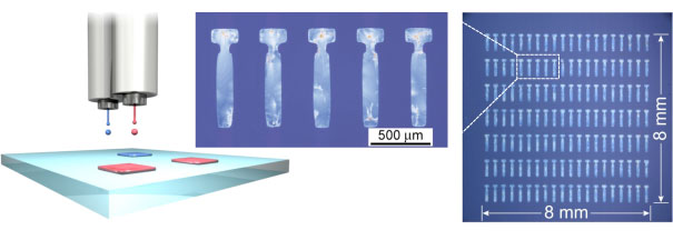
Figure 1: Single-crystal thin films of organic semiconductors formed at respective positions by a new inkjet printing technique
|
Social Background of Research
The printing technology, which is used to reproduce characters or pictures such as photographs on papers, now attracts considerable attentions in the field of electronics, since it can be utilized as a new manufacturing technology for electronic devices by the print production of fine electronic circuits at micrometer resolution on a sheet. For example, replacing a vacuum film-formation process and lithography by the printing technology should make large-scale and high electricity-consuming vacuum facilities unnecessary in the production of large-area electronic devices such as flat displays. Furthermore, the use of plastic sheets should lead to the flexible electronics products as characterized by light-weight, thin, and impact-resistant features, which would revolutionize the future electronics industry.
In order to realize such a printable electronics technology, it is necessary to produce TFTs, indispensable building blocks for large-area electronics products such as flat displays, by a printing method. In particular, it is now the central issue to improve the performance of TFTs produced by a printing method. Semiconductors are known to perform at the high enough level only if the constituent atoms and molecules are ordered regularly. Therefore the main challenge for the success of printable electronics technology is to find out a way to form highly uniform semiconductor layers from the deposited microliquid droplets by a printing technique on the surface of sheets.
History of Research
AIST has been promoting the research and development of the printable electronics technology in a wide range of aspects. A part of the research and development has focused on organic semiconductors that are most suitable for the printable electronics technology, since many organic semiconductors are soluble in organic solvents and can be processed at ambient pressure and temperature. It is known for organic semiconductors that high-mobility devices are obtained by using highly-crystalline low-molecular-weight organic materials. However, it is difficult to control the crystallization of semiconductor materials in solution due to the convection flow and random crystallization inside the droplets, so that it has been considered to be extremely difficult to form a uniform semiconductor layer by conventional printing techniques. In this study, the researchers developed the double-shot inkjet printing technique which uses alternating print deposition of microliquid droplets both of ink composed of a dissolved organic semiconductor and of another ink that prompts crystallization of the organic semiconductor, and succeeded in producing single-crystal thin films of organic semiconductors with molecularly flat surfaces. The organic semiconductor material, C8-BTBT, used for producing single-crystal thin films was provided by Nippon Kayaku Co. Ltd. The X-ray diffraction measurements of the semiconductor single-crystal thin films were conducted using synchrotron radiation at the Photon Factory of KEK.
This study is supported by the New Energy and Industrial Technology Development Organization through a Grant for Industrial Technology Research (FY 2008 - 2012) and also by the Japan Society for the Promotion of Science through its FIRST Program, "Quantum Science on Strong Correlation" (FY 2009 - 2013).
Details of Research
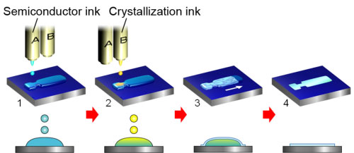
Figure 2 shows a schematic of the double-shot inkjet printing technique to produce semiconductor single-crystal thin films. Two kinds of ink are used, namely the semiconductor ink composed of the dissolved organic semiconductor C8-BTBT and the crystallization ink which prompts crystallization of the organic semiconductor. The crystallization ink is first deposited from an inkjet head, and the semiconductor ink is then overprinted from another inkjet head on the deposited crystallization ink to form an intermingled microliquid droplet (whose total volume is 3 nanoliter) on a sheet. A supersaturation state of the organic semiconductor is immediately formed in the intermingled droplet, which results in the slow film growth of the organic semiconductor at the droplet surface. The semiconductor layer eventually covers the entire droplet surface. The obtained thin film is 30 - 100 nm in thickness, depending on the printing conditions such as ink concentration, is highly uniform, and has a molecularly flat surface. Furthermore, it is possible to control the growth direction of the semiconductor layer by forming an appropriate deposited pattern through the hydrophilic/hydrophobic surface treatment of the sheets. All the process temperatures for producing the single-crystal thin films are below 30 °C. Thus the semiconductor thin films with highly uniform thickness were produced at arbitrary positions reproducibly, which was extremely difficult by the conventional printing techniques (Fig. 1).
 |
|
Figure 2: Schematic of semiconductor single-crystal thin film production by the double-shot inkjet printing technique |
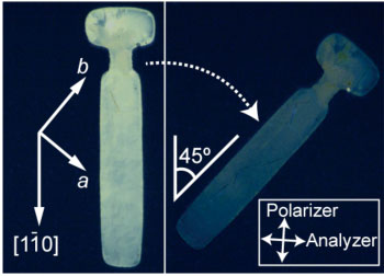
The synchrotron X-ray study was performed for the films, and it was found that all the diffractions were observed as clear spots (Fig. 3). The result clearly indicates the high crystallinity of the films. The refined unit cell based on the analyses of the observed Bragg diffractions is also consistent with that of C8-BTBT. Additionally, the films were investigated by a crossed-Nicols microscope that is suitable for the observation of anisotropic crystals. It was found that the color of almost the entire film uniformly changes from bright to dark, when the film was rotated around an axis perpendicular to the film surface (Fig. 4). The results imply the single-domain characteristic of the semiconductor thin films. Furthermore, stripes with intervals of several micrometers to several tens of micrometers were observed in the optical microscope and the atomic force microscope images of the films (Fig. 5). The stripes are associated with the steps having the height of one molecular layer of C8-BTBT, and can be ascribed to the step-and-terrace structure that is characteristic of the semiconductor single-crystal thin films.
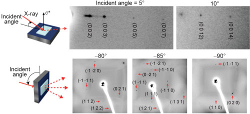 |
Figure 3: X-ray diffraction photographs of the organic semiconductor single-crystal thin film
Out-of-plane (top) and in-plane diffractions (bottom) |
 |
|
Figure 4: Crossed-Nicols polarized microscope images of the organic semiconductor single-crystal thin film |
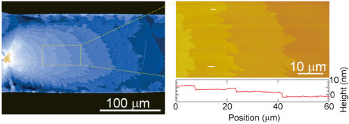 |
Figure 5: Optical microscope (left) and atomic force microscope (right)
images showing the step-and-terrace structure on the organic semiconductor single-crystal thin film |
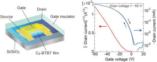
Field-effect transistors were fabricated by forming source and drain electrodes (Au) and a gate dielectric layer (an organic polymer film) on the single-crystal thin film of the organic semiconductor (Fig. 6 left). The mobility of the devices in the saturation region reaches the maximum value of 31.3 cm2/Vs and 16.4 cm2/Vs on average. The mobility is more than 10 times as high as that of amorphous silicon TFTs (about 1 cm2/Vs) that are used in commercial liquid-crystal displays, is 100 times as high as that of organic TFTs fabricated by conventional printing methods, and is the highest among organic TFTs. The on/off current ratio is 105 - 107, and the subthreshold slope was about 2 V per decade with a threshold voltage of about 10 V. Hardly any current hysteresis was observed in the transfer and output characteristics, where the shift in the threshold voltage from forward to reverse sweeps was less than 0.1 V. The characteristics were not degraded by more than 10 % after the films were kept in air for 8 months.
As presented above, the newly-developed double-shot inkjet printing technique, using the alternating print deposition of two types of microliquid ink droplets, is quite useful for manufacturing organic semiconductor thin films with high uniformity and for improving the performance of the TFTs using the films considerably: both have been the main challenges in the printable electronics technology.
 |
|
Figure 6: Schematic of the field-effect transistor structure and the measured transfer characteristics
|
Future Plans
The researchers will further optimize the printing conditions, semiconductor materials, and device structures, and improve the device performance and stability. They also plan to manufacture high-performance active backplanes with the whole printing processes, by combining the various printing techniques such as printing of metal wires, electrodes, and others.