- III-V/Ge CMOS transistors with more than 200% mobility enhancement against Si CMOS transistors -
We have successfully demonstrated the III-V/Ge CMOS transistors with InGaAs n-channel and Ge p-channels integrated on the one wafer by direct wafer bonding (DWB) for the first time. The mobilities of III-V/Ge CMOS transistors exceeded more than 200% against the Si CMOS transistors. This is the important step for realizing next generation high-performance III-V/Ge CMOS transistors.
The University of Tokyo, UT, (President: Junichi Hamada), National Institute of Advanced Industrial Science and Technology, AIST, (President: Tamotsu Nomakuchi), Sumitomo Chemical Co. Ltd., SC, (President: Masakazu Tokura), and National Institute for Materials Science, NIMS, (President: Sukekatsu Ushioda) have studied III-V compound semiconductor and III-V-on-insulator (III-V-OI) transistors which are compatible with Si platform.
In this work, we have developed the key technologies for realizing high-performance III-V/Ge CMOS transistors; (1) integration of III-V channels on Ge wafers and demonstration of high mobility III-V/Ge CMOS transistors with self-align Ni-based metal source/drain (S/D) process (UT), (2) enhancement of electron mobility in extremely-thin body (ETB) III-V-OI MOSFETs (UT), and (3) III-V/Ge CMOS technique with common metal S/D and gate electrodes (AIST).
We present these accomplishments as three papers at “2011 Symposia on VLSI Technology” (VLSI symposia 2011) (June 13–16, 2011, Kyoto, Japan).
This work has been supported by Innovation Research Project on Nano electronics Materials and Structures from NEDO since 2007.
♦Point♦
We have successfully developed III-V/Ge CMOS transistors with more than 200% higher electron and hole mobilities than the Si CMOS transistors. In addition, we have developed high electron mobility ETB InGaAs-OI MOSFETs and scalable III-V/Ge CMOS technique with common metal S/D and gate electrodes. These results can allow us to realize the next generation high-performance III-V/Ge CMOS transistors.
Point 1: The world’s first demonstration of high-performance III-V/Ge CMOS transistors
-
We have successfully demonstrated the III-V/Ge CMOS integration of InGaAs-OI nMOSFETs and Ge pMOSFETs with self-align Ni-InGaAs and Ni-Ge metal S/D on a Ge substrate, by using DWB technique, for the first time. InGaAs-OI-on-Ge wafers with Al2O3 buried oxide (BOX) layers have been developed by DWB technique. Ni-based metal S/D allows us to fabricate InGaAs-OI nMOSFETs and Ge pMOSFETs at a single-step S/D formation process. The fabricated InGaAs-OI nMOSFETs and Ge pMOSFETs have exhibited the higher electron and hole mobilities than those of Si MOSFETs by more than 200%, respectively. This result will open up the way to realize the high-performance III-V/Ge CMOS transistors for logic LSI.
Point 2: High mobility ETB III-V-OI nMOSFETs with InGaAs composite channels
-
We have successfully demonstrated high electron mobility in the ETB III-V-OI nMOSFETs with approximately 10-nm-thick InGaAs composite channels, for the first time. The InGaAs composite channel InGaAs-OI nMOSFETs show more than 400% higher mobility than Si nMOSFETs.
Point 3: Scalable III-V/Ge CMOS technology with common metal S/D and gate electrodes
-
We have successfully developed scalable III-V/Ge CMOS technology with common metal S/D and gate electrodes and III-V/Ge CMOS operation with the gate length of less than 100 nm have been demonstrated for the first time.
♦Summary♦
Summary 1: The world’s first demonstration of high mobility III-V/Ge CMOS transistors
~Integration of high electron mobility III-V channels and high hole mobility Ge channels on the one wafers by DWB technique and self-align Ni-based metal S/D III-V/Ge CMOS process~
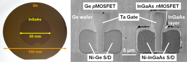
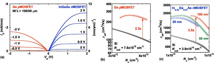
We have successfully developed InGaAs-OI-on-Ge wafers with atomic-layer-deposition Al2O3 (ALD-Al2O3) BOX layers by ALD-Al2O3 assisted DWB technique, for the first time, as shown in Fig. 1-1(a). In addition, we have developed the self-align Ni-based metal S/D process for fabrication of III-V/Ge CMOS transistors on the one wafer, as shown in Fig. 1-1(b). As a result, we have demonstrated the InGaAs-OI nMOSFETs and Ge pMOSFETs integrated on the one wafer, for the first time, as shown in Fig. 1-2(a). And we have found that the integrated InGaAs-OI nMOSFETs and Ge pMOSFETs show the higher electron and hole mobilities than Si transistors, as shown in Fig. 1-2. The hole and electron and hole mobilities and the mobility enhancement against Si is ~ 260 and ~ 1800 cm2/Vs and ~ 2.3 × and ~ 3.5 ×, respectively, as shown in Figs. 1-2(b) and (c).
 |
|
Fig. 1-1 (a) Photograph of a III-V-OI-on-Ge wafer. A 2-inch InGaAs layer has been successfully transferred on a 4-inch Ge wafer. (b) InGaAs-OI nMOSFET and Ge pMOSFET fabricated by self-align Ni-based metal S/D process. |
 |
|
Fig. 1-2 (a) Electrical transport properties InGaAs-OI nMOSFETs and Ge pMOSFETs fabricated on the InGaAs-OI-on-Ge wafer. The normal transistor operation of both InGaAs-OI nMOSFETs and Ge pMOSFETs was confirmed. The mobility properties of (b) the Ge pMOSFETs and (c) InGaAs-OI nMOSFETs. The mobility enhancement against Si transistor is 2.3 × for Ge pMOSFET and 3.5 × for InGaAs-OI nMOSFET, respectively. |
Summary 2: Development of high electron mobility ETB III-V-OI nMOSFETs
~ Development of the InGaAs composite channel III-V-OI MOSFETs with 1-nm-thick effective channel ~
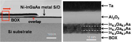
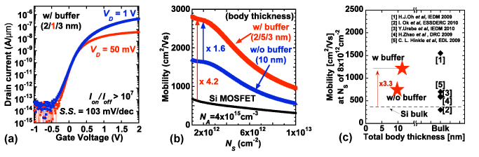
We have developed ETB III-V-OI nMOSFETs with ~ 10-nm-thick InGaAs composite channels, for the first time. InGaAs composite channels have a channel layer of InGaAs with high In content (an effective channel layer) and buffer layers of InGaAs with low In content. The channel layer is sandwiched by the MOS interface buffer layers. Here, the current flows the channel layer of InGaAs with high In content because of the difference in band offset. Therefore, the scattering of carriers at the MOS interfaces can be suppressed, as a result, the mobility can increase even in the ETB structure. The high quality epitaxial ~ 10-nm-thick InGaAs composite channels were grown by Sumitomo Chemical Co. Ltd. We have fabricated the ETB InGaAs-OI MOSFETs, and we found the high quality channel transfer as shown in Fig. 2-1. Figure 2-2 shows the electrical transport properties of an ETB InGaAs composite channel III-V-OI nMOSFETs. We have successfully demonstrated the transistor operation of an ETB InGaAs composite channel III-V-OI nMOSFET even with the effective channel thickness of 1 nm, as shown in Fig. 2-2(a). Furthermore, we have demonstrated the higher mobility in an ETB InGaAs composite channel III-V-OI nMOSFET than Si transistors by 4.2 ×, as shown in Fig. 2-2(b). As a result, we found that the mobility of the ETB InGaAs composite channels III-V-OI nMOSFETs is as high as that of the bulk III-V MOSFETs, as shown in Fig. 2-2(c). The high mobility ETB InGaAs composite channel III-V-OI nMOSFETs are promising for scaling because the ETB structures can suppress the short channel effect.
 |
|
Fig. 2-1 Cross-sectional micrograph of ~ 10-nm-thick InGaAs composite channel III-V-OI nMOSFET. The InGaAs composite channel composed of channel layer of InGaAs with high In content and two buffer layers of InGaAs with low In content. The current flows in the channel layer. |
 |
|
Fig. 2-2 Electrical transport properties of III-V-OI nMOSFETs with InGaAs composite channels. (a) Demonstration of InGaAs composite channel III-V-OI nMOSFET with the effective channel thickness of 1 nm. (b) Mobility properties of InGaAs composite channel III-V-OI nMOSFET with the 5-nm-thick effective channel and 10-nm-thick InGaAs single channel III-V-OI nMOSFET. The InGaAs composite channel III-V-OI nMOSFETs shows mobility enhancement of 4.2 × against Si. (c) The benchmark of the electron mobility. The mobility of the ~ 10-nm-thick ETB InGaAs composite channel III-V-OI nMOSFETs is as high as that of the bulk III-V nMOSFETs. |
Summary 3: Development of scalable III-V/Ge CMOS technology with common metal S/D and metal gate electrodes
We have successfully developed scalable III-V/Ge CMOS technology with common metal S/D and gate electrodes and III-V/Ge CMOS operation with gate length of less than 100 nm have been demonstrated for the first time.
Figure 3-1 shows the band lineup of InGaAs and Ge. The conduction band edge of InGaAs and the valence band edge of Ge are located near the work function of midgap metal in Si technology. Therefore, we can use common gate electrodes for n/pMOSFETs from the view point of controlling the threshold voltage. In addition, this gate electrode is suitable for metal S/D in Schottky barrier S/D transistor operation. As a result, we can commoditize both metal S/D and gate electrodes. In this work, we used TaN as common metal in Schottky barrier InGaAs/Ge n/pMOSFETs. Figure 3-2 shows a cross-sectional micrograph of the fabricated InGaAs nMOSFET with the gate length of 50 nm. As shown in Fig. 3-3, we have demonstrated the InGaAs nMOSFET and Ge pMOSFET with the gate length of 100 nm for the first time, and the symmetric transistor operation has been achieved. We found that the developed process using common metal S/D and gate electrodes can allow us to realize the scaling of the III-V/Ge CMOS performances with simple process.
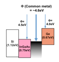
Fig. 3-1 Band lineup of InGaAs and Ge
|
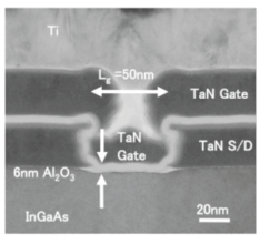
Fig. 3-2 Cross-sectional micrograph of InGaAs nMOSFET with the gate length of 50 nmBand lineup of InGaAs and Ge
|
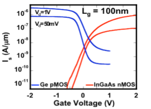
Fig. 3-3 Electrical transprt properties of InGaAs nMOSFET and Ge pMOFSET with the gate length of 100 nm fabricated by the common process
|
As mentioned above, we have developed the high mobility III-V/Ge CMOS transistors for logic LSI. In addition, for further improvement, we have developed ETB InGaAs composite channel III-V-OI MOSFETs and scalable III-V/Ge CMOS process with common metal S/D and metal gate electrodes. These key technologies for future generation III-V/Ge CMOS transistors can allow us to enhance the performance and reduce the energy consumption of the computers.
History of our project
In our project, we have proposed the alternative channel materials and new engineering process in order to develop transistors for 16 nm generation. Especially, we have focused on the III-V compound semiconductors because of their high electron mobility and light electron mass. Recently, we have successfully developed 3.2- to 100-nm-thick InGaAs-OI nMOSFETs on Si substrates with SiO2 or Al2O3 BOX layers by DWB process, with leading the world. We have already demonstrated the high mobility InGaAs-OI nMOSFETs even with the InGaAs channel thickness of less than 10 nm compared to Si transistors. We have reported our achievements in 2009 Symposia on VLSI Technology, 2010 Symposia on VLSI Technology, 2010 International Electron Device Meeting, and so on up until now.
In this work, we have successfully integrated the high electron mobility III-V channels and high hole mobility Ge channels and demonstrated the III-V/Ge CMOS transistors for the world’s first. We present this work in 2011 Symposia on VLSI Technology.
“2011 Symposia on VLSI Technology” (VLSI symposia 2011) (June 13–16, 2011, Kyoto)
The date of release is at 8 a.m. on June 12, when the proceedings release.
TODAI TLO, Ltd. And Sumitomo Chemical Co. Ltd. applied for a patent concerning this matter.