Shigeru Niki (Leader) and Shogo Ishizuka (Research Scientist) of Thin Film Compound Semiconductor Team, Research Center for Photovoltaics (Director: Michio Kondo) of National Institute of Advanced Industrial Science and Technology (President: Hiroyuki Yoshikawa) (hereinafter referred to as AIST) developed a Thin Film Technology which can subdue the consumption of selenium raw materials below one-tenth of the conventional standard at the time of manufacturing of non-silicon-based CIGS thin film solar cells. Due to this, it is possible to expect mass production of high performance CIGS module.
CIGS solar cells use Cu (In, Ga) Se2 (Copper, Indium, Gallium, 2 Selenium: CIGS) as the light absorption layer. It has attracted attention due to the possibility of decreasing the thickness of the photoelectric conversion layer to a few µm, and theoretical conversion efficiency exceeds that of a single crystalline silicon solar cell. The multi-source evaporation process is effective for the production of high performance CIGS thin films, but as the efficiency of selenium was low by this method, technical control of thin films and reduction of cost was difficult, thereby making it unfit for industrial use. By forming radicals from vapor selenium, and raising their reactivity compared with the conventional selenium vapor deposition method, we succeeded in improving the efficiency of selenium consumption by more than 10 times.
The details of the research results were announced in the Materials Research Society Spring Meeting held in San Francisco (U.S.A.) 9th-13th of April, 2007.
 |
|
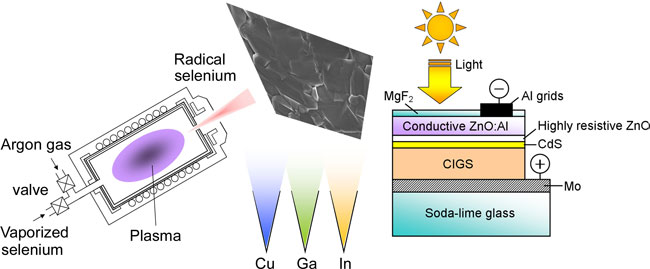
Figure 1. Schematic illustration of the CIGS film growth using a Se-radical beam source and solar cell structure.
|
The conversion efficiency of solar cells is an important performance index directly related to the cost, and there are big expectations for high performance solar cells, which can generate sufficient electricity even within a small area, because of the world energy situation.
A CIGS solar cell has (1) high conversion efficiency (highest of 19.5% with a thin-film solar cell was achieved by National Renewable Energy Research Laboratory, U.S.A.) (2) a superior long-term reliability as it doesn't wear out due to long-term usage (3) a soothing black color (4) superior resistance to radioactive radiation, etc. those are distinguishing characteristics compared to the conventional silicon based solar cells. On this account, technology for mass-production of CIGS solar cells has been undertaken and efforts are on to launch a new solar cell industry. The multi-source evaporation is known for the high conversion performance CIGS thin film manufacturing process, but as this method uses the heated vaporized selenium which is difficult to handle, problems such as consumption of large quantity of selenium and frequent maintenance of the production system is required. These problems become factors to hinder the mass production of CIGS thin film. Therefore, development of technology for higher control towards manufacturing of low selenium consuming CIGS solar cells was awaited.
Till now, on the basis of CIGS thin film technology using the multi-source evaporation method in AIST (1) development of in situ observation and technical control of growth (2) development of solar cell manufacturing process suitable with wide gap CIGS (3) development of technology for control of crystalline defects in CIGS thin film etc. has been undertaken. In the Research Center for Photovoltaics, research is not only limited to small area solar cells but also research for increasing the efficiency of integrated modules has been undertaken. The technology verified in small area solar cells has been applied in the research related to high performance of the module quickly.
This research was sponsored by NEDO (New Energy and Industrial Technology development Organization), with support from "Research and Development for high-efficiency technology of large area CIGS solar cell (2006-2010)".
Various ways have been proposed regarding the manufacturing method of CIGS thin film till now, but selenization methods and multi-source evaporation methods are most promising. Selenization is a method to form CIGS thin film by heating metal precursor layers such as copper, indium in a hydrogen selenide gas chamber to make CIGS solar cells. This method does not produce solar cells of high conversion efficiency as the multi-source evaporation method produce, but it is widely used as a technology for the production of large area CIGS thin film. On the other hand, the multi-source evaporation method is a process to vaporize elements such as copper, indium, selenium and it has an advantage to achieve high conversion efficiency of small area CIGS solar cells at laboratory level. As this method consumes large quantities of selenium, the development of large area/mass production technology is considered to be difficult.
In the multi-source evaporation method, it is necessary to supply metal raw materials such as copper, indium, gallium and several tens of selenium raw materials during the production of thin film. In this process, usual vaporized selenium consists of comparatively large molecules such as Se2, Se5, Se6, Se7, Se8, with low reactivity. And there is a need of high temperature for the production of thin films, and selenium atoms re-vapor from the carefully made thin film surface due to high temperature. These are the cause for such high consumption of selenium. Due to these, most of the selenium sticks and accumulates in the inner walls of the vacuum chamber and are disposed as industrial waste. Also, frequent maintenance of the production device is necessary. As this raises the cost of CIGS solar cells, it is assumed unsuitable as a mass production technology.
We developed a technology for the purpose of better control and efficient use of selenium raw materials in the multi-source evaporation method at the AIST. We replaced conventional vaporized selenium with selenium radicals made by the RF plasma cracking to produce CIGS thin films. With this technology, on/off control of selenium supply during production of thin film can be possible. As high reactivity of radical selenium can be utilized, we succeeded in controlling consumption of raw materials to one-tenth the amount of the conventional vaporized selenium. This also means that we were able to improve safety in handling selenium.
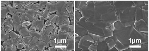
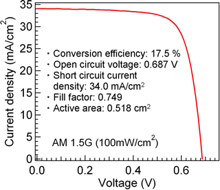
Metal raw materials, except selenium, still use the same conventional vapor of Knudsen-cell source. It is found the CIGS thin film produced in this new technology using radical selenium shows a smooth and dense surface and has large grains. The small area solar cells made with this CIGS thin film technology shows high conversion efficiency as conventional CIGS solar cells do.
 |
|
Figure 2. Scanning Electron Microscopy images of the surface of CIGS films grown with a conventional Se-evaporative source (left) and a Se-radical beam source (right).
|
 |
|
Figure 3. Current-voltage curve of a solar cell using CIGS absorber grown with a Se-radical source.
|
Along with examining the application of radical selenium in the production of large area modules of CIGS thin film, application of the technology in the following areas firstly, wide gap CIGS thin film with high gallium density, improvement of efficiency of solar cells, and development of low temperature thin film technology are under way. In addition, this unique CIGS thin film made by radical selenium has the advantage of a large grain size with a smooth surface, and along with raising the stability and reliability of the thin film growth, we are challenging to achieve a higher performance device.