- Development of a technique to fabricate very low-cost radio frequency ID tags -
The National Institute of Advanced Industrial Science and Technology (AIST) has developed a method which can drastically reduce the electrical resistance of antennas, wirings etc., of radio frequency (RF) ID tags formed by screen printing. This method is one where, after printing the antenna and wiring with metallic inks, a pressure annealing process is applied to them without high temperature baking. Using this technique, we have succeeded in fabricating RF ID tags on flexible substrates entirely by printing. This indicates that high-sensitive RF tags can be formed on flexible substrates such as plastics entirely by printing, and thus a further reduction in the cost of the tags can be facilitated. This will induce the acceleration of widespread use of the tags.
RF ID tags are terminals which give and receive information by RF signals, by which existence of and information about objects can be recognized and administrated. Because of their convenience, widespread use of the tags is expected, but their high manufacturing cost is an obstacle at present. Thus the establishment of low-cost fabrication techniques of the tags is urgently needed. Techniques for fabricating the tags entirely by printing have been investigated to resolve this problem, but none have been established yet.
We have developed a "pressure annealing" technique to reduce the resistance of conducting circuits formed on plastic film substrates by printing, without high temperature baking. Antenna circuits created by this method showed a sensitivity similar to that of antennas produced by a commercial vacuum processing technique. Moreover, using our technique, we have confirmed that RF ID tags fabricated entirely by screen printing, applying our technique, can work well at frequencies of 5-40 MHz.
The pressure annealing method is applicable to the fabrication of the wirings and electrodes on flexible substrates, such as plastic films, by printing, because even if the baking of conducting inks is done at temperatures below 200°C, their resistance can be sufficiently lowered. We expect that the method developed may be applied for various devices to manufacture low-cost, flexible ubiquitous information terminals.
A part of this study was presented at the 66th Meeting of the Japan Applied Physics Society in autumn 2005, held from September 7 to 11 in Tokushima Prefecture.
Recently, RF ID tags have attracted a great deal of attention as information terminals which can administer information of objects. They can give, receive, and control information about the objects by RF waves without being in contact with detectors, and can also be remotely-controlled, and they can display their ability for immediate administration of object information. Already, the tags are partially being used routinely, e.g., in the electronic toll collection systems of various transportation facilities. For convenience, RF ID tags have been purposed to be applied to price and baggage tags of general products to administrate their prices and logistics, but the high manufacturing cost of the terminal devices is an obstacle to promoting their widespread use.
Thus, if the RF ID tags can be fabricated entirely by printing, they can be prepared together with commercial products (to which the tags are attached) at the time of fabrication, as well the bar codes used at present, and a substantial manufacturing cost reduction can be expected. However, many problems still remain, without sufficient perspective. For example, the devices need to be formed on film substrates such as plastics, because the products to which the devices are attached have various shapes, and in addition they are often distributive ones. Component materials for the RF ID tags, such as conductive inks, mostly require a high temperature baking process after printing to obtain high conductivity. However, for the substrates of general-purpose plastics, the high temperature processing is not applicable to them; the temperature is, at the highest, 200°C. Thus, so far, it has been difficult to make good use of devices fabricated entirely by printing.
We have developed a technique which can reduce the resistance of conductive materials printed on substrates as antennas and wirings without high temperature baking. Furthermore, applying this technique, we have developed a method to fabricate RF ID tags by screen printing. The techniques are explained below.
When antennas, wirings, and electrodes are printed, the materials of the inks must be conducting. Metallic pastes, such as silver, gold, and carbon pastes, and organic conducting polymers which have solvent-solubility, are currently known conductive inks. However, as the resistance of the organic conducting polymers is very high, the metallic pastes are used for the antenna and wiring of the RF tags, which must have low impedance.
As various treatments, e.g., metal fracturing to fine particles, and binder mixing, are done to make metal paste inks, a baking processing is needed to reduce their resistance. In particular, the usual metal pastes require a high temperature (400-500°C) baking to obtain sufficiently high conduction, indicating that they are not applicable to general-purpose plastic film substrates, which cannot endure heat processing above 200°C.
In this work, we have found that the resistance of the metallic pastes can be reduced by a low temperature baking below 200°C if the annealing is done under pressure. We formed electrodes on plastic films by screen printing with silver pastes, and baked them at 150°C. The resistance of the electrodes was measured before and after the pressure-annealing processing; the resistance of the pressure-annealed electrodes was reduced by more than three orders of magnitude compared with that of the electrodes prior to the processing. When the processing is not done, the filling factor of the metallic powder in the conductive ink is low because of the baking at a low temperature of 150°C, resulting in high resistance, while, when the processing is done, the filling factor increases reducing the resistance.
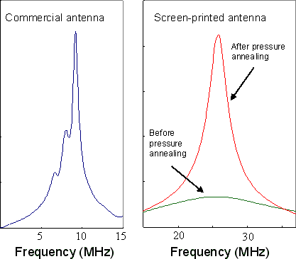
Figure 1 shows the RF frequency characteristics of an antenna before and after processing using our technique, and that of an antenna formed by a commercial dry process. The frequency characteristics usually exhibit a sharp peak at the frequency resonant with signal RF waves. The frequency characteristic curve of the antenna without the processing has a broad peak, and its signal response is low because of its high impedance.
However, for the pressure-annealing processed antenna, its frequency characteristic curve has a sharp resonant peak similar to that of an antenna formed by a commercial dry process, because the RF wave response increases due to the reduction in the impedance. The frequency range of the RF wave used is between 5 and 40 MHz. On the other hand, the frequency of IC cards used in the transport facilities is 13.56 MHz, and thus the pressure-annealed antenna can display its power around the standard frequency.
 |
|
Figure 1 Left: Frequency characteristic of commercial antenna (formed by vacuum processing). Right: Frequency characteristic of antenna formed by our method. |
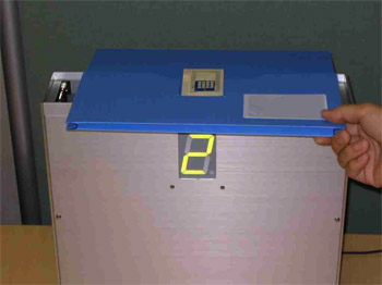
Using an antenna printed by the technique we have developed, a passive-type RF tag was formed on a plastic film, and an operation check of the tag was done at frequencies of 5-40 MHz with a commercial RF ID tag reader. Figure 2 shows a photo image in which the operation of the RF ID tag, formed by the entirely printed method, and attached to a holder (blue entity), is checked by approaching a tag reader (white box) (see Fig.2). The identification number, 2, of the holder (blue entity) was displayed in this check, indicating that the individual information of the holder was recognized. Thus, this demonstrates that the ID tags fabricated by the printing work well.
 |
|
Figure 2 A holder (blue entity), to which the printed tag is attached, approaches a tag reader (white box) for recognition. |
The frequencies used for the operation check in this work are 5-40 MHz, which correspond to the standard operation frequency (135 kHz or 13.56 MHz) for electromagnetic induction type RF ID tags. This indicates that our technique is applicable to standard RF communication systems.
The technique we developed in this work can be used not only for RF ID tag fabrication but also for the formation of the wiring on plastic substrates by printing. We also hope that the technique is applicable to the fabrication of a variety of flexible devices.
This study was adopted as a task force item of the AIST Innovation Center for Start-ups for a project of "Strategic Research Rationale Promotion" on the basis of the outlays for promoting science and technology of Ministry of Education, Culture, Sports, Science, and Technology, and carried out with the support of the Center.