The Nanoelectronics Research Institute (NeRI) of the National Institute of Advanced Industrial Science and Technology (AIST), an independent administrative institution, has succeeded in fabricating ferroelectric gate transistors by a self-aligned-gate technique which enables down-sizing. The ferroelectric gate transistor is expected to be the new generation of non-volatile semiconductor memory device. We have demonstrated that an ON/OFF drain current ratio greater than 105 was held for 10 days after data writing.
This successful study makes the down-sizing possible for a ferroelectric gate transistor, which was difficult for a conventional non-self-aligned-gate ferroelectric transistor. This study will accelerate the development of single transistor FeRAM.
♦ Long-Time Data Retention of Self-Aligned-Gate Ferroelectric Transistor
The new generation non-volatile semiconductor memory of a ferroelectric gate transistor is superior to a generally-adopted flash memory in points of high endurance against many write cycles and high-speed writing. The ferroelectric gate transistor also has other merits such as requiring very little write-current, using only one transistor for a single FeRAM cell and obeying scaling-rules for transistors, and non-destructive data readout. However, the ferroelectric gate transistor used to show a short data retention time because of difficulty in selecting proper materials and keeping good quality in fabrication process.
The NeRI-AIST has already succeeded in demonstrating excellent data retention characteristics of a non-self-aligned-gate ferroelectric transistor fabricated by preparing source and drain regions on a silicon (Si) substrate prior to forming of a metal-ferroelectric-insulator-semiconductor (MFIS) stacked structure (AIST Press Release, October 24, 2002, and other reports). In a non-self-aligned-gate ferroelectric transistor, the stacked structure under the gate electrode can be protected from possible damages caused by etching and ion implantation. However, the non-self-aligned-gate ferroelectric transistor has difficulty in down-sizing by obeying scaling-rules for transistors. Therefore, a prospective use of a ferroelectric gate transistor as a practical non-volatile semiconductor memory will require the self-aligned-gate technique. Now our self-aligned-gate ferroelectric transistors succeeded in showing large ON/OFF drain current ratio over 105 even after 10 days of retention time, in which source and drain regions were formed by ion implanting over the gate stacked structures. This successful study is a major breakthrough in application of ferroelectric gate transistors to practical one-transistor-type nonvolatile memory.
♦ Development of Insulator Materials Most Suitable for Ferroelectric Gate Transistor
Complex oxide of strontium, bismuth and tantalum (SrBi2Ta2O9 or SBT) used in this work has good endurance and is one of the most intensively studied ferroelectric materials for memory device applications. The SBT requires being polycrystallized by high-temperature annealing in order to show ferroelectricity. When the SBT is used in an MFIS ferroelectric gate transistor, all the other layers in the MFIS stacked structure are inevitably heated up to the high temperature at the same time of the SBT annealing. If an insulator layer in the MFIS ferroelectric gate transistor is polycrystallized by the high-temperature annealing, a leakage current through the insulator layer is increased. The increase of the leakage current through the insulator layer can degrade retention characteristics of the MFIS ferroelectric gate transistor, therefore, the insulator layer should be resistant to the polycrystallization. Moreover, the insulator layer should be made of high-permittivity (k) material so that an effective voltage applied on the ferroelectric layer in the MFIS structure can be as large as possible, because the voltage applied on the gate electrode is the sum of effective voltage applied on every layer in the MFIS structure. The NeRI-AIST has intensively studied hafnium (Hf)-aluminum (Al)-oxygen (O) complex oxides, which are made of HfO2 and Al2O3, as good candidates for the insulator material in the MFIS structure, because it has the two significant characters of the resistance to polycrystallization at high temperature and the high permittivity. This time, we succeeded in finding the optimum ratio of Hf and Al in HfAl-O complex oxides for the insulator-layer application in a MFIS ferroelectric gate transistor, which enables us to reproduce excellent ferroelectric gate transistors with long memory retention.
This successful work was reported on December 15 at the 2004 IEEE International Electron Devices Meeting (IEDM2004) held at San Francisco, U.S. December 13 through 15, and three patents have been filed in relation to the present work.
Recently, ferroelectric random access memory (FeRAM) has been intensively researched and developed as one of competing non-volatile semiconductor memories. In comparison to flash memory, which is the generally-used non-volatile semiconductor memory now, FeRAM has certain advantages such as high endurance against many write cycles and high-speed writing. In addition, the FeRAM has smaller power consumption than MRAM, which is rapidly-developed non-volatile memory in very recent years, because there is no intrinsic need of a large write current for memorizing the FeRAM to ‘1’or ‘0’ by switching ferroelectric polarizations. Currently manufactured FeRAMs are categorized as 1T1C, 2T2C, and so on, where T and C mean transistor and capacitor, according to the number of the control transistors, T, and the memory capacitor(s, C, in a memory cell. Every ferroelectric memory capacitor is fabricated apart from the control transistor in these types of FeRAM. These types of FeRAM require rewrite operations after read-out of ‘1’or ‘0’ data because they lose the data every time they are read. Further more, the prospective down-sizing of these FeRAMs are restricted by keeping a large area for the several transistors and capacitors in a single memory cell. On the other hand, an FeRAM made of ferroelectric gate transistors needs only one transistor per one memory cell, shows non-destructive read-out operations, and have a potential of much down-sizing. The ferroelectric gate transistor is a kind of field effect transistor (FET), where the gate oxide layer is replaced by two layers of a ferroelectric and a buffer insulating layers. The buffer insulating layer is prepared in order to prevent Si diffusion into the ferroelectric layer. Such an excellent ferroelectric gate transistor, however, has many technical problems in the fabrication which include difficulties in material selection. Therefore the practical use of the ferroelectric gate transistor as a memory device has not been realized for long time ever since the basic conceptions of the ferroelectric gate transistor have been proposed.
The NeRI-AIST has succeeded in extending the data retention time by using complex oxide including hafnium for the insulator layer of the MFIS gate structure (AIST Press Release, October 24, 2002, and other reports). However, the early ferroelectric gate transistor had a problem of down-sizing because of the non-self-aligned-gate structure. As a result of further R&D efforts, the new self-aligned-gate ferroelectric transistor showed excellent data retention characteristics, which indicate feasibility for a practical use of the ferroelectric gate transistor as the coming generation non-volatile memory applied to semiconductor integrated circuits.
(1) Development of Insulator Materials for Ferroelectric Gate Transistor and Optimizing of the Composition Ratio
By using a high-k material as an insulator layer in an MFIS stacked gate structure, a voltage distribution to a ferroelectric layer becomes relatively large. The large voltage applied on the ferroelectric layer results in a large ferroelectric polarization, which increases ON/OFF drain current ratio by widening a memory window in drain current versus gate voltage hysteresis curves. The ON/OFF drain current ratio is an important factor of good retention characteristics. As the other important factor, a long retention time can be obtained by keeping a leakage current through the insulator layer small enough. In this study, a Hf-Al-O complex oxide was used as the insulator layer in the MFIS stacked gate structure. The Hf-Al-O is made of high-k HfO2 and Al2O3, which is expected to suppress a leakage current through the insulator layer by resisting a polycrystallization. As a ferroelectric layer, we used an SBT deposited by a laser evaporation technique, which shows good and reproducible ferroelectricity. We prepared many ferroelectric gate transistors with Pt/SBT/(HfO2)x(Al2O3)1-x/Si MFIS stacked gate structures, in which many Hf-Al-O with various composition ratio were used in the insulator layers. We also prepared many gate oxide transistors with Pt/(HfO2)x(Al2O3)1-x/Si MIS gate structures, in which many Hf-Al-O with various composition ratio were also used in the insulator layers. All of the MFIS and the MIS transistors were investigated. As a result, the Hf-Al-O with the ratio of about HfO2 : Al2O3 = 3 : 1 showed a large permittivity and no polycrystallization even after a high temperature O2 annealing at 800oC for 1h, which is the necessary annealing condition for the SBT crystallization. The ferroelectric gate transistor, which has the Hf-Al-O insulator layer with the proper ratio of HfO2 : Al2O3 = 3 : 1, showed very good memory retention characteristics. The study demonstrated that the Hf-Al-O material with the ratio of HfO2 : Al2O3 = 3 : 1 is suitable for the insulator layer in the ferroelectric gate transistor in case of using the ferroelectric SBT together.
(2) Fabrication of Self-Aligned-Gate Ferroelectric Transistor with Long-Time Data Retention
Source and drain regions were made by self-aligned-gate technique which was applied on the MFIS stacked gate structure fabricated on the basis of the work (1). The self-aligned-gate technique is roughly as follows. At first, gate regions on the metal-ferroelectric-insulator stacked layer were masked by photoresist and patterned by lithography. Next, the stacked layer with the photoresist films on the gate regions was etched by ion beam. At last, source and drain regions were formed by phosphorus ions (P+) implanting over the metal-ferroelectric-insulator-semiconductor staked gate structure in order to complete the process of fabricating the ferroelectric gate transistor (Fig.1 and Fig.2). A drain-current versus gate-voltage curve is shown in Fig.3, which is characterized as a hysteresis loop drawn by ferroelectric polarization switching. Good retention characteristics with a large ON/OFF drain current ratio of the self-aligned-gate ferroelectric transistors were demonstrated for the first time as shown in Fig. 4. This study indicates that we could succeed in avoiding possible damages to the ferroelectric gate transistors, which are caused by the etching for forming the gate-stacks and also by the P+ implantation for making the source and drain regions. As for a self-aligned-gate ferroelectric transistor with a gate length of 2µm, where 1µm = 1/1000000 m, a large ON/OFF drain current ratio over 105 was confirmed after 10 days of retention time since the '1'or '0' data was written. Drain-current retention characteristics for the other self-aligned-gate ferroelectric transistors with gate lengths of 3µm, 5µm, and 10µm, were as good as the one with a gate length of 2µm, as indicated in Fig. 4. (In Fig.4, the horizontal axis means how long time passed after the'1'or '0' data was written. The vertical axis means how large the drain read current, Id, is, when a little drain read voltage was applied. Both axes were drawn in logarithmic scale. A large drain-current ratio of ON- to OFF- states results in a reliable distinction between 1' and '0' data. Therefore, the ON/OFF drain current ratio of the ferroelectric gate transistor gives an estimation of a quality of retention characteristics. The ferroelectric gate transistor with a gate length of 2µm showed an ON/OFF drain current ratio over 107 immediately after the data writing, which was after 1 s precisely, and kept a very large ON/OFF drain current ratio over 105 after 10 days-long retention time. The drain current ratio over 104 is expected after 10 years of retention time by extrapolating the two ON and OFF-state curves in Fig. 4. )
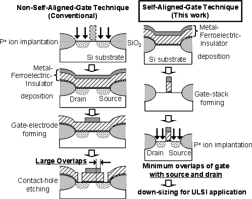 |
Fig. 1 Comparison of fabrication processes for ferroelectric gate transistors by non-self-aligned-gate and self-aligned-gate techniques. |
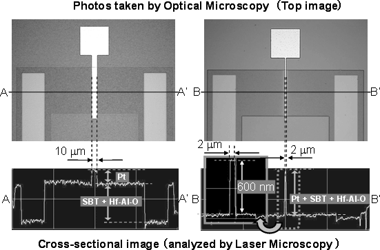 |
Fig. 2 Top and cross-sectional images of ferroelectric gate transistors prepared by using non-self-aligned (left) and self-aligned (right) gate techniques. |
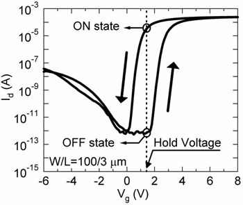 |
Fig. 3 Drain current hysteresis curve of self-aligned-gate Pt / SBT / (HfO2)0.75(Al2O3)0.25 / Si transistor. |
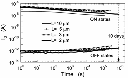 |
Fig. 4 Data retention characteristics of self-aligned-gate Pt / SBT / (HfO2)0.75(Al2O3)0.25 / Si ferroelectric transistors with gate lengths, L, of L = 2µm, 3µm, 5µm and 10µm. All of these devices showed excellent retention characteristics. A long retention time of 10 days was obtained by measuring the self-aligned-gate ferroelectric transistor with the smallest gate length L = 2µm. The write voltages applied on gates of all the devices for ON and OFF states were +8 V and -6 V, respectively. The hold voltage of 1.5 V was applied on the gate of the device with L = 2µm during the retention measurements |
In conclusion, our success in fabricating the self-aligned-gate ferroelectric transistors with good retention characteristics will accelerate a down-sizing of a ferroelectric gate transistor, because a consideration of alignment accuracy in patterning the gate structure by photolithography is not needed by using the self-aligned-gate technique. The down-sizing could not be promoted by using a conventional non-self-aligned-gate ferroelectric transistor because it needs larger gate overlaps than the alignment accuracy in the gate photolithographic process. This work, which first demonstrated good retention characteristics of the self-aligned-gate ferroelectric transistors, therefore made a great step forward in their prospective industrial application to one-transistor-type FeRAM expected as the coming generation non-volatile semiconductor memory device.