- Gbit MRAM is in sight with the realization of 230% magnetoresistance ratio by the use of sputtering method -
National Institute of Advanced Industrial Science and Technology (AIST) (President Hiroyuki Yoshikawa) Nanoelectronics Research Institute (Director: Toshimi Wada) and ANELVA Corporation (President: Aritaka Imamura, 5-8-1 Yotsuya, Fuchu-shi, Tokyo) have successfully developed a mass manufacturing technology suitable for preparing high performance Tunneling Magneto Resistance (TMR) device, which is the core device for high speed non-volatile Magnetoresistive Random Access Memory (MRAM). The novel TMR device, which uses magnesium oxide as the tunnel barrier layer and was successfully developed by AIST in March this year, was fabricated by a sputtering system which is suitable for mass manufacturing. World best performance of 230% magnetoresistance ratio at room temperature has been achieved, which is three times larger than the conventional TMR device. As a result of the great leap of magnetoresistance ratio, the signal output could be doubled to 370 mV compared to that of the conventional TMR. Based on industrial experience, this higher signal output is large enough in fabricating next generation high-density MRAM devices that may extend well over Gbit range. The much higher magnetoresistance ratio of the newly developed TMR device also facilitates in manufacturing of more sensitive magnetic heads. This assures in realizing hard-disk drives with increased recording density; a vital feature to develop “ambient intelligent” that yet to come.
To date, the novel TMR device could only be fabricated by using highly sophisticated technology, such as molecular beam epitaxy (MBE). However, the MBE process is so complex that it limits the mass manufacturing capability of TMR devices. On the other hand, the current result demonstrates that high performance novel TMR device can be prepared by an existing sputtering system suitable for mass manufacturing of MRAM.
MRAM (Magnetoresistive Random Access Memory) is a memory device which relies on magnetism instead of electrical charge to store data as that in DRAM(Dynamic Random Access Memory) (Fig.1). Scientists around the world have been developing the MRAM as an alternative replacement for DRAM, due to its fast operation and high-density capability. Furthermore, MRAM maintains stored data even after the power is turned-off (non-volatility) and is well suited for applications in harsh environments. Therefore, it is considered as the ideal memory.
Motorola and IBM have been leading the MRAM development. Motorola shipped its first 4 Mbit MRAM chips to select customers in late 2003. Meanwhile, IBM group announced the development of 16 Mbit MRAM in June 2004. In Japan, NEC and Toshiba began the MRAM development in 2003 in a framework of National Project after receiving funding from Japanese government.
The current technology of MRAM gives magnetoresistance ratio about 70% at most, and an output signal lower than 200 mV. Even with this technology, it is expected that MRAMs with memory capacity as high as 64 – 128 Mbit can be fabricated. The lower value of output signal becomes an issue in increasing MRAM density as the signal is buried by noise and cannot be retrieved when the density is further increased. Therefore, a substantial improvement of TMR, the core component of MRAM, is necessary to realize MRAM with higher densities (Fig.2).
To solve this problem, scientists around the world have put a lot of efforts to optimize the material of ferromagnetic electrode and fabrication method of tunnel barrier layer, aluminum oxide. However, in principal, this conventional method to increase the magnetoresistance ratio and signal output has reached its limit. Therefore, drastic measures to realize Gbit-scale high-density MRAM are necessary.
The upper limit of magnetoresistance ratio of TMR device using aluminum oxide as the barrier layer is considered to be around 70%. To overcome this limit, a novel TMR device utilizing magnesium oxide as the tunnel barrier layer has been proposed and studied by many researchers. Aluminum oxide is an amorphous material (the atoms are in disorder state). As a result, the electrons are scattered making it difficulty to proceed straight through the barrier layer (Fig.3(a)). On the contrary, since magnesium oxide is in a single-crystal state ( the atoms are in ordered state), the electrons can move straight without suffering dispersion (Fig.3(b)).In this case, theoretical study predicts that huge tunnel magnetoresistive effect is resulted.
Experimental results related to the novel TMR devices, particularly the rising of magnetoresistance ratio have been reported since 2001. In spring 2004, AIST announced that it has succeeded in surpassing the magnetoresistance ratio of the conventional TMR device by realizing a novel TMR device with magnetoresistance ratio of 88% at room temperature. The result has attracted a good deal of attention (Fig.4). However, the novel TMR device was fabricated on special substrate (magnesium oxide substrate) rather than on Si substrate which is indispensable in LSI manufacturing process. Furthermore, it was deposited using a special ultra high vacuum evaporation system, which yields low productivity. In general, ultra high vacuum evaporation system has several technology disadvantages such as: short maintenance cycle, bad controllability of material composition and difficulty in miniaturization of hardware. Therefore, it is thought that the novel TMR device cannot be mass-produced for practical applications. Therefore, it is thought that the novel TMR device cannot be mass-produced for practical applications.
(1) Mass production technology to fabricate novel TMR device on Si substrate has been realized using sputtering machine (world’s first)
ANELVA started the development of mass production technology for the novel TMR device after AIST successful experimental confirmation this spring. Taking account of the process applicability for magnetic-head or MRAM production process, sputtering deposition method is utilized instead of ultra-high vacuum evaporation technique. The sputtering system used during this study is based on a mass production system for magnetic-head or MRAM production. The sputtering system has a unique feature of wide distance and offset configuration between the substrate and the target (material source for deposition) (Fig.5). Furthermore, compared with conventional sputtering system the sputtering gas pressure can be reduced by one order. As the result, high-energy sputtered atoms, which bombard and cause microstructure disorder, can be suppressed and films with smooth surface and superior properties can be obtained. Using this technique, we have successfully fabricated the novel TMR device, which shows excellent properties, on 8 inch diameter Si wafer used for MRAM production (Fig.6). From the cross-section micrograph of transmission electron microscope, we can see that very smooth magnesium oxide layer grows on the Si substrate (Fig.7).
(2) Novel TMR device with 230% huge magnetoresistance ratio at room temperature (world’s highest performance)
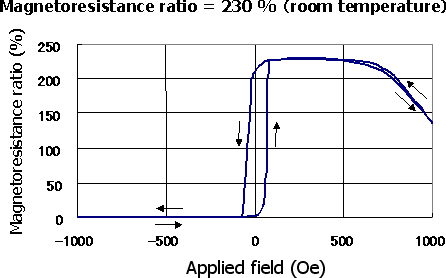
Magnetoresistance ratio is a typical parameter to evaluate the TMR device performance. To date, the highest magnetoresistance ratio of TMR device using aluminum oxide as the barrier layer is around 70%. It is considered that the magnetoresistance ratio of the conventional TMR device has reached its theoretical limit and improvement of its performance cannot be expected. On the other hand, on March 2004, AIST made a landmark by surpassing the magnetoresistance ratio of the conventional TMR device by realizing a novel TMR device with magnetoresistance ratio of 88% at room temperature. This time, by fabricating a novel TMR device on Si substrate using sputtering technique, world’s highest magnetoresistance ratio of about 230% at room temperature has been obtained (Fig.8).
 |
|
Fig. 8. Magnetoresistance curve of the novel TMR device at room temperature |
(3) A path to realize Gbit-scale MRAM
At present, highly competitive development on conventional MRAM is performed around the world. However, since the highest magnetoresistance ratio value in conventional TMR is 70% at most, the signal output is kept at a level lower than 200mV. As the result, using this technology, MRAM with storage capacity exceeding 64 - 128 Mbit is considered difficult to be realized.
This time, since a novel TMR device which shows huge magnetoresistance ratio of 230% has been successfully fabricated, a signal output of 370 mV is achieved. The signal output level is about twice larger than the conventional TMR device that uses aluminum oxide. This value is almost satisfy the requirement in Gbit-scale MRAM. We believe that further improvement of the film properties can increase the signal output even further.
From the point of view of data access speed, it is required that the resistance of the TMR device in the range of 500-10000Ωµm2. It is worth to note that the novel TMR device that has been prepared this time fulfilled this requirement. It is believed that the present high-performance novel TMR device fabricated by sputtering system suitable for mass production, is a breakthrough to realize Gbit-scale MRAM.
(4) Application of the technology to magnetic-head for high recording density hard-disk drive
To further increase the recording density of hard-disk drive, engineers are trying to integrate the conventional TMR device, which uses aluminum oxide barrier layer, to magnetic-head. Therefore, the currently developed novel TMR device, which was fabricated utilizing an existing sputtering system used for TMR head production and shows much superior magnetoresistance ratio performance as compared with the conventional one, can contribute to the increase of the hard-disk drive recording density through improvement of magnetic-head performance. Note that the required resistance of TMR device for magnetic-head is much smaller than that of the MRAM, in the range of 0.5-4Ωµm2. To reduce the resistance of the presently developed TMR device, reduction of the magnesium oxide thickness, while maintaining the magnetoresistance ratio, will be the next development issue.
The results presented here are a part of collaboration research work conducted by AIST and ANELVA. The samples fabrication was performed at ANELVA, while the micro-processing and evaluation were done at AIST.
Below are the issues to be developed within the framework of collaboration research.
-
Improve the performance of the presently developed novel TMR device
-
Apply the currently developed process to actual MRAM production
-
Clarify the electron transport mechanism of the novel TMR device fabricated by sputtering technique
-
Develop a technology to reduce the resistance of the TMR device for magnetic-head application