- It is possible to produce ultrafine wiring of a few microns in width on the desktop -
The Nanotechnology Research Institute of the National Institute of Advanced Industrial Science and Technology (AIST), has developed a sub-micron ink-jet technology that makes it possible to dispense sub-femtoliter dots 1/1000 smaller than the dots produced by currently available technologies. Applying this technology, we have succeeded in producing highly accurate arrangements of dots, less than one micron in diameter, of diverse materials, such as electroconductive polymers or ultrafine metal particles. (Figs. 1 to 3).
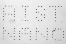
Fig.1 A example of fine characters using sub-micrometor diameter dots.
(dot pitch 3-micrometer)
|
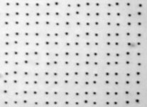
Fig.2 A example of fine lattice pattern using sub-micrometor dots.
(dot pitch 3-micrometor)
|
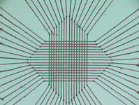
Fig.3 Fine circuit of conducting polymer.
(line width 3-micrometor, 10-micrometor pitches at lattice area)
|
Also, cooperative research on the use of NanoPasteTM of stably dispersed metallic nano particles as a ink material has been carried out with the Tsukuba Research Laboratory of Harima Chemicals, Inc. (hereinafter Harima Chemicals) which developed the ink material (Fig. 4). As a result of this research, we have succeeded in performing direct printing of ultra fine wiring with a few microns width on a given substrate, which is considered a crucial factor in the development of surface mounting technology (Fig. 5). Ultrafine wiring carried out at atmospheric conditions on the desktop is poised to revolutionize surface mounting technology, leading to further miniaturization of electronic devices, whose development and manufacturing demands will be sharply increased.
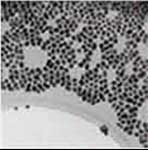
Fig.4 TEM image of "thenanopaste".
(particle diameters are around 5-nanometers)
|
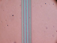
Fig.5 A example of fine pattern using "the nanopaste".
(line/space=3.6/1.4-micrometers)
|
Moreover, this technology can be applied not only to surface mounting related technologies but also to innovative applications in other nanotechnology fields such as biotechnology, optical and ultrafine processing technologies.
To deepen the scope of the research, and to expand the range of applications in this field, AIST is engaged in an ambitious joint research program that includes other particles besides the metal nano particles described in this report. This program will trigger active research on nanotechnologies and further expansion of their fields of application.
The revolutionary autonomous ink-jet method developed by AIST allows production and arrangements of dots with a minimum size of less than one micron, which corresponds to sub-femtoliter units in volume. This volume corresponds to a 1/1000 of the volume of the dots dispensed using the ink-jet devices currently on the market, which places this technology at the top of circuit printing technologies in the world. Using this newly developed technology, AIST has confirmed that diverse materials such as nanotubes, electroconductive polymers and ceramics can be used as solutes for the ink. At the same time, tests using NanoPasteTM, stable dispersion of metal particles developed by Harima Chemicals, have been carried out, resulting in successful circuit printing on diverse substrates such as glass or polyimide. This result shows that it is possible to directly print ultrafine metallic wire of only a few microns in width.
Traditional technologies face a myriad of problems with depletion of natural resources, energy consumption, and environmental impact to investment in plant and equipment. In contrast, this new technology can be characterized as required resources in the required amount, meaning that this is an environment-friendly technology in terms of resources and energy savings. As this technology does not require any expensive production facility and the ultrafine process can be carried out on the desktop under atmospheric conditions, it is hoped that it can be applied to the production of revolutionary devices through a printing process, such as electronic ink, organic EL and organic transistors. Moreover, as it also does not require any exposure masking or evaporation masking, the process time is greatly reduced from circuit design to product testing, which will make rapid progress in the speed of development of new devices possible.
The equipment here developed is still at the laboratory level, but it has a simple design and its practical use should be easy. Ink-jet technology that allows printing of sub-micron dots has never been produced until now. This technology will not only be applied to surface mounting technology, which is joint research with Harima Chemicals, but also extended into other nanotechnology related fields such as biotechnology, optics, and ultrafine processing technologies, as well as into diverse industrial and technological fields.
To promote investigation and to extend the area of application, AIST is considering joint research including this topic, and aiming to activate the research field of nanotechnology and to explore fields of application.