Department of Energy and Environment
The World's First Operation-Verification of
a Hybrid Transistor with Integrated GaN and SiC
- NAKAJIMA Akira, HARADA Shinsuke
Advanced Power Electronics Research Center
Released: December 12, 2021
GaN transistor and SiC diodes made monolithic
By building our own integrated manufacturing process line, we have monolithically integrated both a high electron mobility transistor that uses gallium nitride (GaN) and a PN diode that uses silicon carbide (SiC) and were the first in the world to successfully create and verify the operation of the hybrid transistor. This transistor is expected to be applied to electric vehicles and photovoltaic power conditioners that require high-reliability functionality.
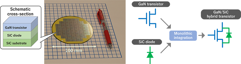 A hybrid-type transistor formed on a 100-mm diameter wafer and its equivalent circuit
Problems with conventional GaN high electron mobility transistors
In order to achieve carbon neutrality by 2050, power converters used in electric vehicles and photovoltaic power generation need to be made more efficient, smaller, and more reliable. Further technological innovation will be also indispensable for power transistors used in power converters. Although GaN transistors are effective in improving the efficiency of power conversion, they have a weak point where they absorb less noise energy when the circuit operates abnormally; this has hindered their widespread use.
Resolving the problem of GaN transistors unable to withstand voltage breakdown during abnormal circuit operation
By designing the breakdown voltage on the SiC side to be slightly lower than that on the GaN side in the hybrid type-transistor we produced, when the breakdown voltage of the SiC diode is exceeded, energy is released as heat on the SiC side, preventing overvoltage on the GaN side; a stable reversible breakdown behavior was confirmed for multiple sweeps. In addition, they were confirmed to have a high drain current of 300 mA/mm and a low on-resistance of 47 Ωmm because the current flows through two-dimensional electron gas in GaN with extremely high conductivity (mobility). In addition, since SiC has three times higher thermal conductivity than Si, excellent heat dissipation characteristics can be obtained with it.
Device operation verification for converters
We are working on verifying the operation of large-area devices with a rating of 10 A or higher that can be used with actual converters. This device technology will lead to higher efficiency and reliability with the next generation of power converters.
Contact for inquiries related to this theme
Power Device Team, Advanced Power Electronics Research Center
NAKAJIMA Akira, Senior Researcher
AIST Tsukuba West, 16-1 Onogawa, Tsukuba, Ibaraki305-8569 Japan
E-mail: adperc_info-ml*aist.go.jp (Please convert "*" to "@".)