Electronics and Manufacturing
Energy and Environment
New Diamond-Silicon Bonding Method May Provide a Glimpse at the Future of Power Semiconductors
- MATSUMAE Takashi
Device Technology Research Institute
- UMEZAWA Hitoshi
Advanced Power Electronics Research Center
Update(MM/DD/YYYY):12/24/2020
Direct bonding in atmospheric air with chemical treatment and 200°C heat treatment
The researchers have developed a technique for direct bonding of the chemically treated surface of a diamond substrate to a silicon substrate in atmospheric air by heat treatment at a relatively low temperature of approximately 200°C.
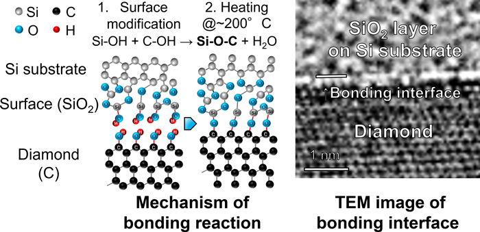 |
| Left: Mechanism of bonding reaction Right: TEM image of bonding interface |
Temperatures of at least 1,000°C or ultra high vacuum have been considered essential
In power semiconductors that control and supply power, diamond is viewed as a promising new material with physical properties that are superior to those of silicon in supporting high efficiency, high output, and modules that are smaller and lighter. To avoid the high cost of manufacturing power semiconductors solely consisting of a diamond substrate, direct bonding of diamond and silicon substrates has been proposed as a way to replace areas that have minimal impact on performance with an inexpensive material. However, conventional direct bonding techniques involve high heat treatment of at least 1,000°C or surface sputter-etching under ultra high vacuum, which requires special equipment.
Enables use of common bonding methods, under precise control of treatment conditions
It is known that substrates chemically modified with hydroxyl groups (-OH) undergo a dehydration reaction when heated to around 200°C and can be bonded by chemical bonds (-O-) between the surfaces (hydrophilic bonding). Through this research, the researchers have developed a technique that enables simultaneous cleaning and hydroxyl group modification of diamond surfaces by using a mixture of sulfuric acid and hydrogen peroxide (H2SO4/H2O2) common in semiconductor substrate cleaning.
Continuing to work toward higher efficiency and smaller, lighter modules
This patent-pending technique has enabled favorable bonding between the (111) surface of diamond and the surface of the silicon substrate, but in future research it will be applied to other crystal planes such as (100) that are easy to synthesize and polish. Bonding with different power semiconductor materials such as SiC, GaN, and gallium oxide (Ga2O3) will also be attempted to investigate application in heat-dissipating or insulating substrates. Other research will attempt polycrystalline diamond bonding and reduction of the SiO2 layer thickness at the bonding interface.
Contact
MATSUMAE Takashi
Researcher
Integrated MEMS Research Group, Device Technology Research Institute
AIST Tsukuba East, 1-2-1 Namiki, Tsukuba, Ibaraki 305-8564 Japan
E-mail: nanoele-web-ml*aist.go.jp (Please convert “*” to “@”)
UMEZAWA Hitoshi
Senior Researcher
Diamond Wafer Team, Advanced Power Electronics Research Center
AIST Kansai, 1-8-31 Midorigaoka, Ikeda, Osaka 563-8577 Japan
E-mail: adperc_info-ml*aist.go.jp (Please convert “*” to “@”)