Department of Electronics and Manufacturing
Developing a Low-Power Magnetometer Capable of
High-Sensitivity and Wide-Band Measurement
- AKITA Ippei
Device Technology Research Institute
Released: February 19, 2022
A magnetometer with 1,000 times the energy efficiency and 1/100th the amount of noise
By applying our uniquely designed integrated circuit for measurements to the magneto-impedance element, we created a magnetometer with low-noise and wide-band characteristics. It can be expected to be used for compact, high-sensitivity, and low-power sensing for things like bio-magnetic and industrial application measurements, etc.
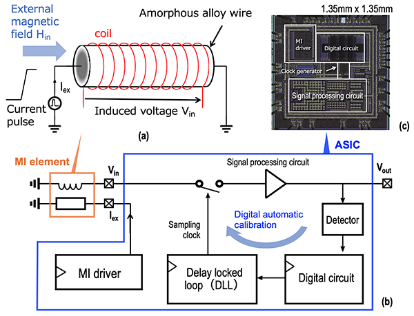 (a) Overview drawing of the MI element. (b) Block diagram of the magnetometer that was developed.
(c) Photo of the ASIC chip for measuring for MI elements.
The challenge of magnetometers for bio-magnetic measurement is simultaneously achieving low noise, low power consumption, and making them compact in size
Low-noise, wide-band magnetometers are required in a wide range of fields, including for biomagnetism for magnetoencephalography and magnetomyography, autonomous driving, non-destructive inspection, and current sensing. The size must be on the order of several millimeters due to restrictions on the amount of space in which it can be placed, and making them compact in size and reducing their weight are particularly necessary for implantable bio-magnetic measurements.
Up to now, small and wide-band magnetometers have tended to increase magnetic noise, and low-noise ones have tended to increase in size and driving current. For applications such as bio-magnetic measurement, the challenge is to achieve low noise, low power consumption, and compact size simultaneously.
A prototype chip incorporating new technique that is confirmed to have low noise and low power consumption
We designed a signal processing circuit that can operate with low noise and low power consumption by constructing and optimizing a new, original circuit for the MI element developed with a joint research company. In addition, in order to control the sampling process of the induced voltage from the MI element by an order of nanoseconds, we have developed a digital automatic calibration technique that monitors the output signal and corrects the sampling timing. By doing this, it is possible to control the noise properties and signal bandwidth at an optimal state.
Integrated circuits used for measurements for MI elements, including the above technologies, were prototyped and evaluated as magnetometers. As a result, it was confirmed that the signal bandwidth and noise characteristics after automatic calibration improved compared to those before the calibration, and that the power efficiency was more than 1,000 times higher than that of conventional low-noise magnetometers.
We will further enhance their performance and move forward with developments to incorporate them as products
As well as further improving their sensitivity and power efficiency as magnetometers, we will proceed with development to incorporate them into products.
Contact for inquiries related to this theme
Advanced Integrated Circuit Research Group, Device Technology Research Institute
AKITA Ippei, Senior Researcher
AIST Tsukuba Central 2, 1-1-1 Umezono, Tsukuba, Ibaraki 305-8568 Japan
E-mail: M-d-tech-web-ml*aist.go.jp (Please convert "*" to "@".)