Researchers) NAKAJIMA Akira, Senior Researcher, HARADA Shinsuke, Team Leader, Power Device Team, Advanced Power Electronics Research Center
- Successful demonstration of monolithically integrated gallium nitride (GaN) transistors on silicon carbide (SiC) diodes
- Solving the overvoltage vulnerability of GaN transistors under abnormal circuit operation
- Promising application to electric power converters for motor driving and photovoltaic power generation, etc.
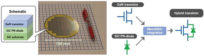
Hybrid transistors on a 100-mm diameter wafer and equivalent circuit
Power converters that control electric energy are important devices that enable energy saving in equipment that uses electric energy, such as home appliances and industrial equipment. Dissemination of electric vehicles, photovoltaic power generation, and other technology is needed to realize carbon neutrality by 2050, and the power converters used in these applications will require even greater efficiency, miniaturization, and reliability than at present. To achieve this, further technological innovation is also essential for the power transistors used in power converters.
Power transistors are used as electrical switches in power conversion circuits, so the following three performances are required.
(1) Low on-resistance to reduce conduction loss in the switch-ON state for highly efficient power conversion
(2) High-speed ON/OFF switching performance to reduce switching loss
(3) Role as a noise energy absorption source under abnormal converter circuit operations
In silicon transistors, which are currently the main type of power transistors, the performances (1) to (3) above have almost reached the material limits. Therefore, R&D has been conducted on power transistors using wide bandgap semiconductors such as GaN and SiC, toward overcoming the Si limits.
A hybrid transistor with monolithically integrated a GaN-based high electron mobility transistor and a SiC-based PN diode, was successfully fabricated and demonstrated by AIST researchers for the first time in the world. The prototype hybrid transistor achieves both the GaN feature of low on-resistance and the proven non-destructive breakdown of SiC diodes. As a result, application of hybrid transistors is expected to power converters for applications that require high reliability, such as electric vehicles and photovoltaic power generation. Going forward, further optimization of the device fabrication process will be promoted to establish a path to practical application.