Update(MM/DD/YYYY):11/11/2009
High-speed Switching of High-voltage, High-power Converter Achieved by Using SiC Diodes
- It will make large-scale power converter systems in social infrastructure very compact -
Points
-
SiC-PiN diodes and Si-IEGTs were combined to achieve switching frequency four times higher (2kHz switching) compared to conventional technology.
-
Prototype single-phase three-level power converter (±5kV-300kVA) demonstrates high-speed switching equivalent to 4kHz.
-
Equipment size is greatly reduced by removing conventionally required insulating transformer and reducing filter capacity.
Summary
Hiromichi Oohashi (Invited Senior Research Scientist), Yasunori Tanaka (Senior Research Scientist), and Hiroshi Yamaguchi (Deputy Director), the Energy Semiconductor Electronics Research Laboratory (Director: Hajime Okumura) of the National Institute of Advanced Industrial Science and Technology (AIST) (President: Tamotsu Nomakuchi), in collaboration with Toshiba Corporation (Toshiba) (Director, President and CEO: Norio Sasaki), Toshiba Mitsubishi-Electric Industrial Systems Corporation (TMEIC) (President: Hideaki Gokoh), Tokyo Metropolitan University (President: Fumio Harashima), and Ibaraki National College of Technology (President: Yukitoshi Tsunoda), have developed a high-voltage, high-power converter using SiC-PiN diodes and Si-IEGTs. In a prototype model (single-phase three-level power converter with DC ±5kV-300kVA), an IEGT switching frequency of 2kHz, which is four times higher than the conventional equipment, is achieved for the first time. This speed is equivalent to 4kHz switching in a power converter system.
The new power converter uses 4x4mm SiC diodes, developed through AIST's technology on large-area, high-speed, low-power-loss SiC-PiN diodes (6kV-class), and Toshiba's Si-IEGTs. In conventional power converter systems using Si-IEGTs and Si diodes, the IEGT switching frequency is limited to about 500Hz because of the limitations of Si diodes. The use of SiC diodes, with their excellent switching characteristics, results in a higher switching frequency (2kHz). The higher switching frequency allowed us to adopt the method of three-level converter instead of conventional multiple series connection; we were able to eliminate the insulating transformer and at the same time reduce the filter capacity. This will realize greatly reduced size of power converter systems (one-fifth compared to a conventional system).
 |
 |
|
Picture SiC-PiN diodes (left) and power converter (right) |
Social Background of Research
High-voltage, high-power converters with high-power devices are an important power electronics technology supporting social infrastructure systems such as for power generation, industrial drives and electric railways. In the quest for a low carbon society, worldwide demand is rapidly growing in the areas of smart grids, mega solar power generation, wind power generation, and rapid rail transit. Technological progress is needed to establish a competitive edge in the environmental industry and strengthen cooperation in environmental technology.
Technical targets for the development of power converters have always been efficiency, size, and weight just like other electronic systems. The core ingredient of high-voltage, high-power converters is high-speed devices with low power loss; however, in conventional Si semiconductor devices, the large power loss due to the switching characteristics of Si diodes tends to limit the switching speed and hinder the improvement of efficiency, size, and weight of converter systems.
To overcome these limitations and meet the global requirements, there is great demand for new technologies that can deliver more efficient use of power in the large-scale converter systems for social infrastructure.
History of Research
In response to this problem, the five institutes participating in the joint research and development project entered into a package deal contract to jointly develop a high-speed switching module through the combined use of high-voltage SiC-PiN diodes with excellent switching characteristics and Si-IEGTs.
AIST has a long history of research and development on power converter technology using SiC and GaN, promising materials for next-generation semiconductor devices; the Power Electronics Research Center (FY2001–FY2007) and the Energy Semiconductor Electronics Research Laboratory (FY2008–present) have continuously pushed the envelope on studies extending from the materials such as crystals to the applications. In the present joint research and development project, AIST is mainly responsible for the technical areas of world-leading high-voltage (6-kV class) SiC-PiN diodes as well as simulators for power loss analysis.
Using their abundant knowledge on semiconductor device fabrication and modularization, Toshiba is responsible for the technical areas of Si-IEGT supply for power converters, module fabrication, and power loss analysis.
TMEIC handles the basic design and testing of power converters, technical areas in which they have extensive knowledge.
Tokyo Metropolitan University, with abundant knowledge on the control of power converters, is in charge of that technical area as well as the cooling design.
Using their abundant knowledge on designing gate drive circuits, Ibaraki National College of Technology is responsible for designing a gate drive circuit to drive Si-IEGT devices with higher switching speed.
The present research and development activities are jointly conducted by pooling the wisdom of these five institutes.
Details of Research
The present research and development project aims at overcoming the technical problem limiting the high-speed operation of power converters. A high speed switching module was developed using high-voltage (6kV-class) SiC-PiN diodes with excellent switching characteristics and Si-IEGTs (Figs. 1 and 2).

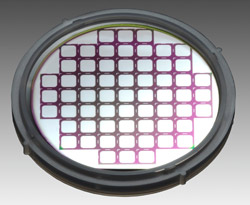
Fig. 1 SiC-PiN diodes; 4x4mm devices on a 2-inch wafer |
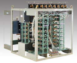
Fig. 2 Set of modules for prototype power converter |
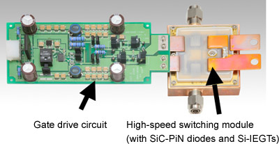
Since the switching frequency is limited by the characteristics of Si diodes in conventional systems, we adopted high-speed, high-voltage and low-power-loss SiC diodes instead of Si diodes in developing a high speed switching module. Large-area (4x4mm) SiC-PiN diodes as realized by the large-area SiC device fabrication technology of AIST, and Si-IEGTs of Toshiba were used for fabricating the switching module, and a cooler and a high-speed gate driving circuit were also developed for the module (Fig. 3).
 |
|
Fig. 3 High-speed switching module and gate drive circuit |
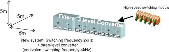
The newly developed high-speed switching module realizes higher-speed driving compared to conventional power converters where only Si semiconductor devices are adopted. Since the devices can be driven faster, we were able to adopt three-level converters instead of a multiple series connection requiring an insulating transformer (Fig. 4). Note that a great advantage of three-level converters is that the output waveform has the equivalent of twice the switching frequency of the devices adopted. Since the output waveform is improved by increasing the switching frequency, large-capacity filters are not required for removing the output waveform distortion. In conventional high-voltage, high-power converters with a multiple series connection, the insulating transformer occupy half the space of the system, and the filters occupy about a quarter of the system, which is really a waste of space. In comparison, the space can be drastically reduced if three-level converters are adopted.
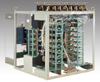
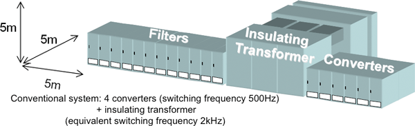
To demonstrate the improvement in switching speed, a test system was prepared with high-speed switching modules of a three-level converter (±5kV-300kVA, Fig. 5), and its performance was tested. Fourfold higher-speed driving (switching speed 2kHz) was achieved compared to a conventional power converter (500Hz) using Si semiconductor devices alone. In three-level converters, we are able to eliminate the insulating transformer and the filter space is also greatly reduced. Our estimation shows that the space is reduced to one-fifth that of a conventional power converter system using Si semiconductor devices alone (Fig. 6).
The developed technology greatly reduces the size and the space of a high-voltage, high-power converter system; this would lead to the wide use of power converters in social infrastructure systems. There is a growing worldwide demand for high-voltage, high-power converters, and the present results are important not only from the viewpoint of establishing a competitive edge in the industry but also from the viewpoint of furthering cooperation in environmental technology.
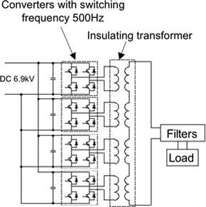
(a) Conventional circuit (with insulating transformer)
(equivalent switching frequency 2kHz)
|
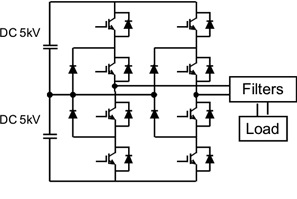
(b) Three-level converter (without insulating transformer)
(equivalent switching frequency 4kHz)
|
|
Fig. 4 Comparison of circuits |
 |
|
Fig. 5 Exterior view of prototype power converter |
 |
|
(a) Conventional system (quadruple series connection with switching frequency 500Hz and insulating transformer) |
|
|
 |
|
(b) New system (three-level converter with switching frequency 2kHz and without insulating transformer) |
|
Fig. 6 Space reduction effect (10MVA-class power converter) |
Future Schedule
The five institutes participating in the present joint research and development will continuously advance the project toward commercial use of the developed technology.