Satoshi Yamasaki (concurrently Principal Research Scientist of the Energy Technology Research Institute) and Norio Tokuda (former Post-Doctoral Research Scientist), the Nanotechnology Research Institute (Director: Nobutsugu Minami) of the National Institute of Advanced Industrial Science and Technology (AIST) (President: Tamotsu Nomakuchi), in cooperation with Satoshi Gonda (Senior Research Scientist) et al. of the Dimensional Standards Section (Section Chief: Toshiyuki Takatsuji), Lengths and Dimensions Division, the National Metrology Institute of Japan (Director: Masahiro Okaji) of AIST have fabricated a nanometer-sized ruler to be used as a primary standard, which is integral to nanotechnology research and production, by taking advantage of the crystal structure of diamond.
Today, research development of new materials and functions is widely advanced making full use of nanotechnology, in which nanometer-sized substance and nanometer level phenomena are studied, and innovative development of science and technology is anticipated. However, the minimum scale of commercially available rulers to serve as a basis of nanotechnology is approximately 10 nm, indicating that a stable and accurate nanometer-sized ruler had not hitherto been materialized. Advancing the diamond film technology as part of research in semiconductor diamond, AIST has succeeded in fabricating a very stable and accurate ruler with a minimum scale of 0.2 nm, which is 1/50 of the one currently available commercially.
The developed ruler is expected to be a global standard of nanometer-sized length, and to contribute to nanotechnology.
The result of the research will be published in online edition of Applied Physics Express, the Japan Society of Applied Physics, on April 17, 2009.
 |
|
Diamond nano-structure with a step height of 0.2 nm |
Science and industrial technologies have to date been developed based on accurately defined worldwide standards of time, length, mass, temperature, etc. Today, technological development in nanometer-sized objects is being pursued in the area of molecular handling technology in biotechnology and VLSI (very-large-scale integration) devices in semiconductor technology. Thus, there is an increasing need for a nanometer-sized ruler. As 1 nm is a length extending only over several atoms, atomic-level control technologies are required to fabricate the ruler and atomic-level stability of the ruler is important. Until our development, there were no ideal nanometer-sized rulers (standard samples) available.
Research development is globally pursued to realize stable nanometer-sized rulers. Practical rulers today are made of silicon, but they are not ideal standards for nanometer-level measurement because of surface oxidation and roughness, and the lack of atomic-level flatness. (See Table 1)
|
Table 1 Comparison of developed ruler and conventional silicon rulers
|
|
|
Diamond is a semiconductor material just as silicon is. High-quality diamond is now available through chemical vapor deposition (CVD) using methane and hydrogen gases, and is actively studied as a material for developing new semiconductor devices.
AIST has long been developing high-performance electronic devices using semiconductor diamond. One of important manufacturing technologies for semiconductor diamond devices is a fabrication technique of flat diamond surface. As diamond is the hardest of all materials, atomic-level planarization had long been believed difficult to achieve. AIST succeeded in obtaining a 0.1-mm-square perfectly flat surface at the atomic level using advanced CVD technology and a particular substrate structure for the diamond film deposition. By forming atomic steps on a flat surface, a new technology is developed for fabricating a nanometer-sized ruler as described in the following.
Regarding the observation of atomic steps, Takashi Tsuno, et al., Sumitomo Electric Industries, Ltd., observed the nanostructures of an atomic step of 0.09 nm ((001) surface) and a triangular 0.2 nm step ((111) surface) on the surface of a diamond.
This research was partially supported by Grant-in-Aid for Scientific Research (20760455) of the Japan Society for the Promotion of Science.
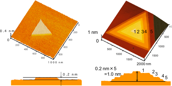
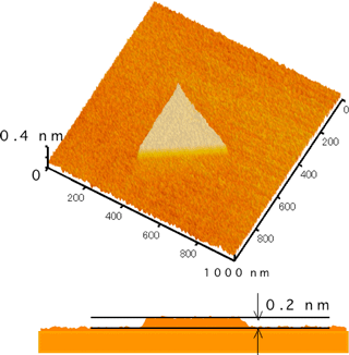
AIST succeeded in fabricating a flat diamond surface at the atomic level by controlling CVD conditions. In this research, it has been found that an island with a step height of one atom can be obtained on a flat diamond surface by subtly changing the CVD conditions. Figure 1 shows the island structure as measured by an atomic force microscope (AFM).
 |
|
Fig. 1 Triangular diamond nanostructure with a step height of 0.2 nm |
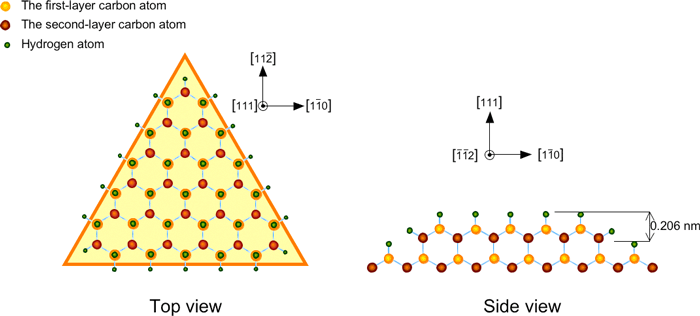
This island consists of a single atomic layer, and the height is accurately determined from the crystal structure of diamond. The distance between adjacent carbon networks in a crystal corresponds to the island height, which is theoretically predicted to be 0.206 nm. Reflecting the carbon atom array structure in a diamond crystal, the island is ideally equilateral-triangular, where the three sides are excellently linear (note: the (111) diamond surface has threefold symmetry). (Fig. 2)
 |
|
Fig. 2 Atomic model of a diamond nanostructure |
As is widely known, diamond is the hardest of all materials, and its structure is barely changed even when the surface is scratched. It is resistant to temperature changes or chemicals, and, unlike silicon, the surface is not oxidized. If the surface is contaminated, a chemical treatment can remove the contaminant, restoring a clean surface. The triangular diamond island as developed has ideal properties for a nanometer-sized ruler: dense structure and physical and chemical stability.
Today, nanometer sizes are measured by using an AFM or a scanning electron microscope (SEM), and the equipment can be calibrated accurately by measuring the developed nanometer-sized ruler. We expect the reliability of nanometer-sized measurements to improve.
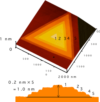
We can further fabricate multi-step equilateral-triangular islands as shown in Fig. 3. We expect the structure to be used as a ruler indicated by an integral multiple of 0.2 nm in the vertical direction, and the ruler in conformity with the size of a measuring object could be fabricated.
 |
|
Fig. 3 Diamond structure with 5 steps (to be used as a standard sample with the height of 1.0 nm)
|
As described above, the equilateral-triangular diamond island fabricated using CVD technology is a promising candidate for a nanometer-height ruler. Further, the length of the three sides, which reflects the crystal structure, can probably be used as another nanometer-sized ruler with unprecedented accuracy.
The fabricated nanometer-sized ruler with a diamond nanostructure will be calibrated with the national measurement standards for length.
Through collaborative studies, we will pursue not only the rulers (standard samples) as developed, but also the possibilities of various electronic devices with diamond nanostructures.