Update(MM/DD/YYYY):06/15/2005
New n-Type Diamond Semiconductor Synthesized
- Opening the Way to Implementation of Diamond-Based Electron Devices -
Key points
-
World-first success in synthesizing (001) n-type diamond semiconductor, of great significance for electron device application.
-
Ultraviolet emitting diode manufactured on trial basis using p-n junction with (001) n-type diamond semiconductor, successfully emitting UV radiation of 235 nm wavelength.
-
A quantum leap toward the practical application of diamond semiconductor, for an electron device.
Synopsis
Dr. Satoshi Yamasaki, a supervising researcher, Dr. Hiromitsu Kato, a researcher, and their colleagues of the Diamond Research Center (DRC), the National Institute of Advanced Industrial Science and Technology (AIST), an independent administrative institution, have succeeded in synthesizing n-type diamond semiconductor on (001) oriented diamond substrate through the vapor deposition leading the world. Furthermore, they have successfully realized ultraviolet emission with UV emitting device prepared on the basis of p-n junction using the (001) n-type diamond semiconductor. This is a very significant achievement eliminating the restriction by the substrate orientation, which has been a bottleneck in the development of electron device derived from diamond semiconductor.
Diamond is characterized by high thermal conductivity, breakdown voltage and very high mobility for electrons and positive holes, to be promising in the application as electron device based on these merits. Particularly, in the area of power device and short-wavelength light emitting device, the highest performance may be expected among various types of semiconductors, and for this reason, a number of research organizations are racing for the development of diamond semiconductor devices.
For implementing electron device based on diamond semiconductor, it is essential to provide both p-type and n-type semiconductors just like for other kinds of semiconductor. While the p-type diamond semiconductor can be synthesized irrespective of the substrate orientation, that of n-type have been available only for (111) oriented substrate, and never for (001). As the n-type diamond semiconductor on (111) oriented substrate provides a lot of difficulties in the commercialization, it has been urgently requested to synthesize on the (001) oriented substrate.
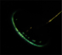
In the present study, the (001) n-type diamond semiconductor has been synthesized through the microwave plasma chemical vapor deposition process using methane as source gas and doping with phosphorus atoms. The success has been ensured by the difference in phosphorus incorporation in the (001) oriented diamond and from that in the (111), by broadly changing conditions for P-doping and by optimizing the synthetic conditions. Moreover, trial manufacture of UV-emitting device has been achieved by using a good preparation of p-n junction on the (001) oriented substrate [Fig. 1, left], and the emission of UV radiation of 235 nm (1 nm = 10-9 m) wavelength has been confirmed [Fig. 1, right]. The UV emission using the (001) n-type diamond semiconductor is also the first success in the world.
Detail of the present work is presented at the 10th International Conference on New Diamond Science and Technology, held from May 11 through 14, 2005. at the AIST Tsukuba Center (Tsukuba, Ibaraki).
|
|
|
 |
|
Fig. 1 UV emission device prepared by use of (001) face n-type diode (left) and UV emission with green light (right)
|
Background
Besides the top value in the family of gems, diamond has a number of merits in some physical properties, such as topmost hardness, exquisite thermal conductivity, extremely high breakdown voltage, broad transmission wavelength band, and superb chemical stability. As a semiconductor, diamond is characterized by high mobility of electrons and holes, and by very small difference between mobility of the two carriers, promising a wide spectrum of applications in electron devices. In particular, the performance of diamond semiconductor-based power device is 15,000 times as good as that of silicon semiconductor, and 10 times that of silicon carbide semiconductor. Besides, light-emitting device made of diamond semiconductor emits radiation of wavelength as short as 235 nm (UV region) much shorter than that of the existing device. For this reason, heated competitions are under way among research laboratories, both domestic and overseas, aiming at the commercialization of electron devices based on diamond semiconductor.
For applying the diamond semiconductor to electron devices, it is essential to develop technology for synthesizing both p- and n-type diamond semiconductors, just like other semiconductors used in devices. Up to now, it has been possible to prepare p-type diamond semiconductor irrespective of crystal orientation by doping with boron. On the contrary, n-type diamond semiconductor has been regarded very difficult to prepare: with successful synthesis achieved only for (111) surface, and not for (001). The (001) oriented substrate is supposed to be ready for being atomically flat surface in principle, taking into consideration of atomic structures in the topmost surface. When attempting the commercialization as semiconductors, the (001) oriented substrate is favored through mechanical polishing, fine patterning and etching of the surface, and yield of such processing, in contrast to the (111) oriented substrate which cannot be atomically flat surface owing to the top hardness among crystal surfaces of the diamond. For this reason, the synthesis of n-type diamond semiconductor has been regarded one of the most important tasks for its application to device preparation.
History of Research Work
The DRC-AIST has been engaged in the study on the element technologies required for the development of diamond-based semiconductors, such as synthesis of high quality diamond semiconductor, synthesis of both p- and n-type diamond semiconductors, as well as control of smoothness for the surface and interface. Besides, the R&D works involve the technologies for wafer development and device preparation, aiming at establishing a consistent process of commercializing the diamond device.
Up to now, a number of significant breakthroughs have been accomplished, such as synthesis of high quality diamond film with atomically flat surface, and successful synthesis of p-type diamond semiconductor film with the highest hole mobility in the world, based on the above-mentioned synthesis technology and doping with boron. Since the foundation of the DRC-AIST, efforts have been concentrated in the development of technology for synthesizing n-type diamond semiconductor.
The present R&D work has been supported by the "Advanced Diamond Device Project (Fiscal Years 2003-05)" under the Development of Materials for Practical Utilization of Nanotechnology, entrusted by the New Energy and Industrial Technology Development Organization (NEDO), another independent administrative organization, and by the "Development of Diamond UV Nanodevices Utilizing High Density Exciton State (Fiscal Years 2001-06)" in "Creation of Nano-Devices and -Systems Based on New Physical Phenomena and Innovative Operational Principle" under the Strategic and Creative Research Promotion Program (CREST Type) of the Japan Science and Technology Agency (JST), still another independent administrative organization.
Details of Research Work
Vapor Deposition Process for Diamond
The diamond semiconductor is synthesized through the microwave chemical vapor deposition (CVD) using methane diluted with hydrogen as source gas. The substrate is prepared on the basis of a diamond mono-crystal board synthesized through the high temperature-high pressure synthesis. The source gas is decomposed by the microwave to a reactive state, and grows to a diamond film through the chemical reaction with the surface [Fig. 2].
|
|
|
Fig. 2 Microwave plasma CVD process for diamond
|
Synthesis of n-Type Diamond Semiconductor and Phosphorus Doping
The n-type diamond semiconductor is synthesized by doping phosphine, a gas containing phosphorus atom (PH3), in the course of diamond synthesis described above. However, the n-type diamond semiconductor has been available for the (111) oriented diamond only. The DRC-AIST has noted that it is of great significance for the synthesis of n-type diamond semiconductor how phosphorus is doped, and in consideration of difference in the way of phosphorus incorporation in for the (001) oriented diamond from that for (111), has identified three key factors for the synthesis of n-type diamond semiconductor, as listed below.
(1) The incorporation efficiency of dopant in for the (001) oriented diamond is lower than that for the (111), and that for phosphorus atom is lower than that for other dopant atoms. For this reason, so long as the same doping conditions for the (111) oriented diamond are applied to the (001) as they are, little phosphorus atoms are incorporated in at the (001) oriented diamond, failing to synthesize the n-type semiconductor.
(2) Incorporation of dopant in the (001) oriented diamond strongly depends on the synthesizing rate, and accelerating the rate can augment the take-in efficiency.
(3) The synthesizing rate affects the formation of surface defects in the course of synthesis, and resultant defects are supposed to inactivate phosphorus atoms. In the (001) diamond, accelerating the rate tends to increase defect formation.
The synthesis of the n-type diamond semiconductor on the (001) oriented substrate has been successfully achieved by optimizing the conditions for synthesis on the basis of adequate understanding and consideration of these key factors (1) through (3), that is, raising the concentration of phosphorus in vapor from hundreds of ppm to as high as a few %, while keeping the synthesizing rate at an appreciable level.
Characterization of n-Type Diamond Semiconductor
The n-type diamond semiconductor is characterized through the measurement of Hall effect, which is the most commonly used method for characterizing the semiconductor. It has been confirmed that the diamond preparation presents the n-type properties stably from the room temperature up to 700 °C or so. The electron mobility at the room temperature is around 350 cm2/Vs, which is comparable to that of (111) n-type diamond semiconductor of nearly identical P-doping level. The concentration of phosphorus taken into the film is estimated to be 2 x 10¹⁸ atoms per cubic cm, with nearly uniform distribution in the depth direction. The next goal for the commercialization of (001) n-type diamond semiconductor is to reduce the electrical resistance further.
Preparation of p-n Junction and Fabrication of UV Emitting Device
When a p-n junction is prepared by using the (001) n-type diamond semiconductor, and a UV emitting device is manufactured on the trial basis, satisfactory junction properties have been achieved. When feeding current into this device, emission of UV radiation of 235 nm has been confirmed [Fig. 3].
|
|
|
Fig. 3 Emission spectrum of trial-manufactured UV emission device
|