- Highest Electron Mobility Achieved in n-Type Organic Semiconductor by Coating with Fullerene Derivative -
The Photonics Research Institute (PRI) of the National Institute of Advanced Industrial Science and Technology (AIST), an independent administrative institution, has successfully prepared n-type organic thin film transistor (TFT) of excellent electron mobility through spin coating process. This achievement is expected to make it possible to produce transistors of large area at low cost, and to accelerate the commercialization of organic devices prepared by printing on flexible substrate such as plastics.
For organic semiconductor materials to be used for organic devices such as organic TFT, organic electroluminescence (EL) device, and solar cell, a number of promising p-type organic semiconductor materials have been known including pentacene of excellent hole mobility and conductive polymer of excellent hole mobility. On the other hand, n-type organic semiconductors of high electron mobility have been found only in limited organic compounds, such as perfluorinated phthalocyanine and fullerene, and for preparing single crystals and thin film of these compounds requires large-scale equipment. Beyond that, preparing through coating process has been thought very difficult.
Fullerene (C60) of soccer ball type construction has been known to have excellent n-type semiconductor properties, and fullerene film prepared in ultra-high vacuum has been known to show electron mobility comparable to that of amorphous silicon. However, with the conventional preparatory process, it has been hardly possible to make large area devices and the process cost has been very expensive. For this reason, the development of innovative coating process has been urgently requested to reduce the production cost and to be applicable to preparation of large-area devices.
The PRI-AIST has succeeded in synthesizing a new fullerene derivative, C60-fused pyrrolidine-meta-C12 phenyl (C60MC12), by incorporating alkyl chain to fullerene (C60). C60MC12 is soluble in organic solvent, and found to constitute a good quality crystalline thin film by simple spin coating where fullerene heads self-aggregate to form layered structure.
An organic TFT has been prepared by using newly synthesized fullerene derivative C60MC12 for organic semiconductor layer, and characterized. The electron mobility is as high as 0.067 cm2/Vs, which is the highest value for n-type organic semiconductor prepared through coating process.
Through the present R&D work, it has been proven to provide, in n-type organic semiconductor prepared by coating, an electron mobility comparable to that of p-type organic semiconductors, which have already achieved a number of successes. In this way, both p-type and n-type organic semiconductors have been made available. This will enhance the degree of freedom in the circuit design using organic semiconductors and accelerate the practical application of smaller-sized organic electron circuits. Besides, organic semiconductors with higher electron mobility will provide valuable spin-off effects to applications for solar cells and memory devices.
For the application of thin film devices based on organic semiconductors, the organic electroluminescence (EL) has been attracting attentions. As commercialization products, the organic EL devices have been adopted in small-sized displays for mobile phones and personal digital assistance (PDA) by some Japanese manufacturers. Currently, R&D works for organic devices based on organic semiconductors have been actively pursued including applications for organic TFTs and solar cells, in consideration of commercialization.
There are two types of semiconductors, as distinguished by the electric sign of carriers: p-type with electricity carried by holes of positive charge, and n-type by free electrons of negative charge. In case of organic semiconductors, while a number of p-type materials have been known such as pentacene with high hole mobility and conductive polymers with high hole mobility, n-type organic semiconductors with high electron mobility have been limited to perfluorinated pentacene with electron-withdrawing elements attached at molecular terminals and fullerene. Among them, fullerene (C60) of soccer ball- like construction is known to have highest electron mobility despite its simple structure. In fact, it has been found recently that high quality thin film of fullerene (C60) prepared under ultra-high vacuum has electron mobility comparable to that of amorphous silicon [Fig. 1]. However, the preparation of crystalline thin film of fullerene (C60) needs the use of ultra-vacuum equipment which is expensive and hardly controllable. For reducing the cost and manufacturing devices of larger area, it is urgently required to establish thin film preparing technology through coating process. However, as fullerene (C60) is difficult to dissolve in organic solvent, preparation of high quality thin film through the spin coat process seems to be very difficult.
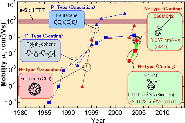
Fig. 1. Mobility of holes and electrons in p-type and n-type organic semiconductors, respectively
On the other hand, in the study of organic thin film solar cells, it has been found that mixed film consisting of n-type organic semiconductor of fullerene derivative, ([6,6]-phenyl C61-butyric acid methyl ester, PCBM) and p-type organic semiconductor, soluble conductive polymers shows high photoelectric conversion efficiency, that is, energy conversion efficiency for simulated solar radiation. This fullerene derivative, PCBM, has been highlighted as n-type organic semiconductor soluble in organic solvent.
However, the characterization of organic TFT made from fullerene derivative PCBM has proved that the electron mobility is as low as 0.023 cm2/Vs. This may be attributed to the fact that the coating becomes amorphous owing to poor self-aggregation of PCBM failing to create charge-carrying channels.
The PRI-AIST has been engaged in materials design for n-type organic semiconductor which is soluble in organic solvent and forms oriented structures by self-aggregation in coating process such as spin coating. Consequently, it has been found that a newly synthesized fullerene derivative, (C60-fused pyrrolidine-meta-C12 phenyl: C60MC12) with 12-carbon alkyl chain incorporated to fullerene (C60) is soluble in organic solvent and has fullerene heads oriented by self-aggregation.
Using fullerene derivative C60MC12 as organic semiconductor layer, n-type organic TFT, i.e., C60MC12-organic TFT, has been prepared through spin coating process and characterized. The technical details are described below.
(1) The C60MC12-organic TFT prepared in this study is of top contact type structure with source-drain electrodes arranged on organic thin film [Fig. 2]. The device has been prepared by spin-coating on a silicon wafer possessing thermally oxidized insulator layer with organic semiconductor layer of fullerene derivative C60MC12. Subsequently, gold is vapor deposited as source and drain electrodes in a vacuum deposition chamber, with 20 mm channel length (source-to-drain .spacing) and 5 mm channel width (effective length of electrode).
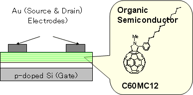
Fig. 2. Structures of C60MC12-organic TFT and fullerene derivative C60MC12
(2) The C60MC12-organic TFT showts good n-type characteristics immediately after preparation, but the heat treatment following the preparation has been found to upgrade the characteristics further [Fig. 3].
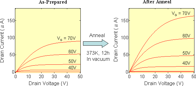
Fig. 3. I-V Characteristics of C60MC12-organic TFT
(3) The transistor output characteristics have been compared between the C60MC12- organic TFT and PCBM-organic TFT prepared in similar way as a reference specimen, to determine the electron mobility. The electron mobility of C60MC12-organic TFT has been as high as 0.067 cm2/Vs, much higher than that of PCBM-organic TFT, 0.023 cm2/Vs [Table 1]. This value is the highest in n-type organic semiconductor prepared by coating process. The current on/off ratio for switching device property is as high as 1.6 x 10⁵.
|
Devices |
Electron Mobility
(m: cm2/Vs) |
on/off ratio |
|
PCBM-organic TFT |
0.023 |
7 x 10⁴ |
|
C60MC12-organic TFT |
0.067 |
1.6 x 10⁵ |
Table 1. Comparison of properties between C60MC12-organic TFT and PCBM-organic TFT
(4) In order to identify the difference in transistor output characteristics between two fullerene- based devices: C60MC12-organic TFT and PCBM-organic TFT, the surface configuration and structural analysis have been carried out by atomic force microscopy (AFM) and X-ray diffraction, respectively. While PCBM film remained amorphous after the heat treatment, C60MC12 has been found good crystalline film with fullerene heads aligned in layer through self-aggregation of appropriately incorporated alkyl chains [Fig. 4].
(5) It may be claimed, therefore, that for the mechanism of electron transport, the band conduction dominates in C60MC12 with C60 segments regularly arranged two-dimensionally within crystalline grains, and hopping conduction is predominant in PCBM where C60 segments are disposed randomly [Fig. 4].
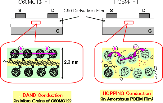
Fig. 4. Molecular Arrangements in C60MC12-organic TFT and in PCBM-organic TFT