- A step towards the realization of 160 Gbit/s optical transceivers able to simultaneously send and receive ultra high-definition images -
Ryoichi Akimoto (Senior Researcher) and others, the Ultrafast Optical Device Research Team, the Network Photonics Research Center (Director: Hiroshi Ishikawa) of the National Institute of Advanced Industrial Science and Technology (AIST; President: Tamotsu Nomakuchi), have developed an ultra-small semiconductor optical gate switching device by monolithically integrating an ultra-high-speed semiconductor all-optical phase modulation device on an indium phosphide (InP) substrate. This modulation device controls the phase of light by using light based on a new principle. Using the developed optical gate switching device, an ultra-high-speed 160 Gbit/s optical signal can be demultiplexed into a 40 GBit/s signal. The device is expected to be used in ultra-high-speed optical transceivers able to simultaneously send and receive ultra high-definition images.
The details of this research will be presented on May 3 at the Conference on Lasers and Electro-Optics (CLEO 2011) to be held in Baltimore, Maryland, USA.
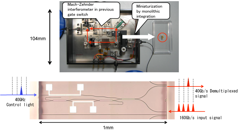 |
Overview : Comparison of size between conventional optical gate switch (top left) and all-semiconductor optical gate switching device miniaturized using
monolithic integration technology (top right).
Micrograph of the developed optical gate switching device and demultiplexing a 40 Gbit/s optical signal from a 160 Gbit/s optical input signal (bottom) |
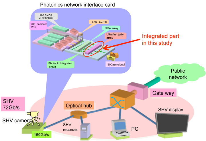
The volume of information transmission has increased rapidly with the dissemination of the Internet, and the construction of optical networks capable of high-capacity and high-speed transmission is an urgent task. In order to realize high-capacity optical communication, transmission speeds per wavelength have been increased to 40 Gbit/s and capacity has been expanded by increasing the number of wavelengths used in wavelength division multiplexing to date. If transmission speeds per wavelength could be further increased, high-capacity transmission would be possible with fewer wavelengths and therefore the miniaturization and the reduction in power consumption of network devices could be expected. Given this, research on multi-level technologies and technologies for ultra-high-speed transmission on the time axis is being actively conducted in order to increase transmission speeds per wavelength. For ultra-high-speed transmission of 100 Gbit/s or more using optical time division multiplexing (OTDM), a technique that renders transmission ultra-high-speed on the time axis, devices using conventional electronic circuits cannot keep up with the necessary signal processing speeds. Therefore, devices that can reduce the speed of transmission to enable processing by electronic circuits are required. The realization of ultra-high-speed optical gate switches that control optical signals using light is the key to the creation of such devices. If a practical, small, and ultra-high-speed optical transceiver that integrated the functions of ultra-high-speed optical gate switches and other devices into semiconductor devices could be realized, we can expect it to enable services such as remote medicine and teleconferencing, which require the transmission and reception of large quantities of data such as high-definition images in real time.
AIST has conducted the development of ultra-high-speed optical gate switching devices using inter-subband transition (ISBT) occurring in quantum wells in an ultra-thin film of a semiconductor material, indium gallium arsenide/aluminum arsenic antimony (InGaAs/AlAsSb). In 2007, in collaboration with the National Institute of Information and Communications Technology, we discovered an all-optical phase modulation effect, a phenomenon related to ISBT, which enables ultra-high-speed control of the phase of light using light. AIST is working on the development of a miniature optical transceiver able to transmit and receive Super Hi-Vision (SHV) signals, in which this all-optical phase modulation effect is applied in optical gate switches. This development is being conducted as part of the “Development of Next-generation High-efficiency Network Device Technology” project (FY2007-FY2011) commissioned by the New Energy and Industrial Technology Development Organization. Figure 1 shows a conceptual diagram of the use of ultra-high-speed optical transceivers at a broadcast station. With the development of optical gate switching modules using a Mach-Zehnder interferometer (see Overview) that employs free-space optics, we have been successful in demultiplexing a 40 Gbit/s signal from a 160 Gbit/s signal. In October 2009, in collaboration with the NHK Science and Technology Research Laboratories, we demonstrated a system that transmitted and received optical time division multiplexed SHV signals.
However, the case of this optical gate switching module was large at 10 cm square, and a complex mechanism was necessary to stabilize the internal conditions of interference. In addition, four gate switching modules were necessary in a transceiver to transmit and receive a 160 Gbit/s signal generated by time division multiplexing of four-channel 40 Gbit/s signals, and coordinating these gate switches was extremely difficult. In order to resolve these issues, we have been working on technologies for the miniaturization and integration of the optical gate switching devices.
 |
|
Figure 1 : Conceptual diagram of optical network using ultra-high-speed optical transceivers |
AIST fabricated an all-semiconductor optical gate switching device for the first time (Overview, Fig. 2), using semiconductor microfabrication technologies to integrate optical waveguides that display the all-optical phase modulation effect due to ISBT and optical circuits forming interferometers on an InP substrate. At 1x0.3 mm2, the surface area of the device is less than 1/10,000 of the 10x10 cm2 surface area of the interferometer section of the previously developed optical gate switching module using free-space optics. Because wafers having a large number of optical gate switching devices can be manufactured in a single dry etching process, the developed devices are highly economical. Laser light sources, optical amplifiers, optical receivers, etc. can also be integrated, and the switching devices are expected to be applied in optical devices having sophisticated functions.
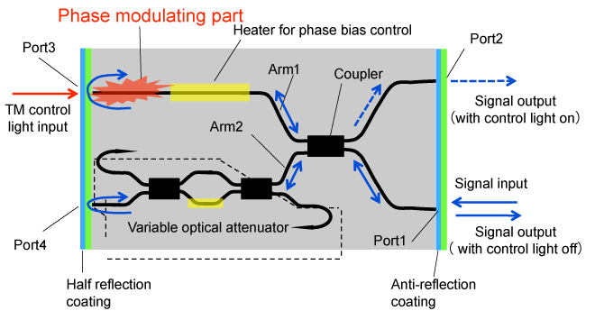
With transverse electric polarized waves that do not exhibit ISBT as signal light, the developed monolithically integrated optical gate switching device uses transverse magnetic polarized waves absorbed by ISBT as control light. The signal light input from port 1 is split in two by a splitter section in the device. Signal light passes through the waveguide in arm 1, the refractive index of which has been changed due to the absorption of signal light by ISBT, and the phase of the light was modulated. This light interferes with the signal light passes through the waveguide in arm 2, the refractive index of which has not been changed. Exploiting the fact that the destination of the interfering signal light changes with differences in the phases of the two signal lights, the optical circuits are designed to output demultiplexed signal light from port 2. This makes it possible to switch the signal light using the control light. As the phase modulation by ISBT is an ultra-high-speed phenomenon occurring in several picoseconds, ultra-high-speed switching is possible. Rather than the previous Mach-Zehnder interferometer, the developed system uses a Michelson interferometer that enables the phase-modulating waveguide section and the section where the control light is introduced to be positioned extremely close to each other.
 |
|
Figure 2 : Configuration of optical circuits in the monolithically integrated optical gate switching device |
Because the optical gate switch uses an interferometer, its switching performance is improved by making the difference in brightness of interfered lights as large as possible. To achieve this, it is necessary to make the strengths of the signal lights for arms 1 and 2 close to each other. When strong control light is absorbed by the waveguide in arm 1, heat is generated causing light loss in the signal light on the arm-1 side, resulting in a breakdown of the balance between light strengths in the arms. In order to avoid this, a variable light attenuator using a Mach-Zehnder interferometer is positioned on the arm-2 side to maintain the even balance between light strengths.
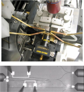 |
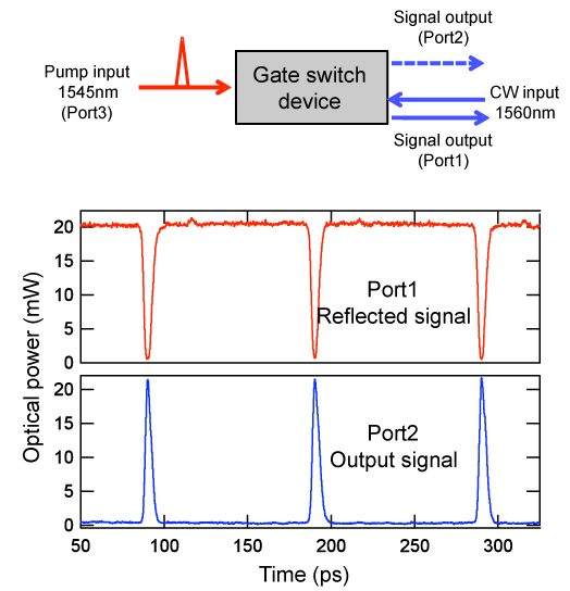
Figure 3 : Evaluation of the optical gate switching device (top)
and Infrared micrograph of the device during evaluation (bottom) |
The operation of the optical gate switching device was evaluated. Figure 3 shows the circumstances of this evaluation. As shown in Fig. 4 (top), continuous transverse electric polarized light with a wavelength of 1,560 nm was introduced from port 1 as signal light, and transverse magnetic polarized light with a wavelength of 1,545 nm, a pulse width of 2.4 ps, a repeat cycle of 10 GHz, and a pulse energy of 8.7 pJ was introduced from port 3 as control light. The lower graph in Fig. 4 (bottom) shows time dependent changes in the strength of the signal light output to port 2, while the upper graph shows the changes in strength of the signal light returning to port 1. Synchronously with the control pulse incident on port 3, part of the signal light input to port 1 was switched at high speed and output from port 2, while signal light returned to port 1 when control light was not incident. The operation of the optical gate switch was clearly verified. When control light was incident under these test conditions, the maximum phase change of the signal light was π radian (corresponding to half the wavelength), and it was confirmed that 100% of the signal light was switched to port 2. The operating duration of the optical gate switch was evaluated from the time waveforms of the signal light output to port 2 and the performance of the switch was confirmed to fulfill the required response speed for an optical gate in an optical transceiver.
 |
|
Figure 4 : Diagram of the switching operation of the optical gate switching device (top); Operating characteristics of the device (bottom): Waveforms over time of signal light returned to port 1 and signal light switched to port 2 |
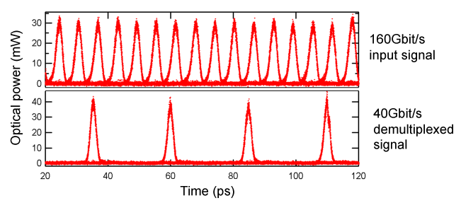
Figure 5 shows the result of demultiplexing one 40 Gbit/s channel from a 160 Gbit/s OTDM signal (a time-multiplexed signal of four 40 Gbit/s signals). This signal processing corresponds to the operation required to isolate and receive a single channel from an OTDM signal of two channels of a full specification SHV signal. A 160 Gbit/s signal is used as the signal light, and a repeating 40 GHz pulse (with a pulse energy of 2.9 pJ) is used as the control light. Adjusting the incidence timing of the control light and coordinating the opening timing of the optical gate with the characteristics of the specific channel of the signal light enabled the signal to be isolated and output to port 2. Zeros and ones were sufficiently distinguishable from the waveform of the output signal, indicating the achievement of high-quality optical gate switching operation.
 |
|
Figure 5 : 160 Gbit/s multiplexed input signal (top) and demultiplexed 40 Gbit/s signal (bottom) |
In future, in addition to increasing the degree of integration of the optical gate switch, it will be necessary to develop integration technologies for pulse light sources, optical amplifiers, optical receivers, and electronic circuits. While developing these element technologies, we aim to ultimately realize ultra-high-speed optical transceivers able to send and receive 160 Gbit/s high-definition images and even faster optical signals without any delay.