Researchers) WANG Xuelun, Laboratory Team Leader, KUMAGAI Naoto, assigned to the team, YAMADA Hisashi, Laboratory Team Leader, GaN Advanced Device Open Innovation Laboratory, SAKAKITA Hajime, assigned to the research institute, SHIMIZU Tetsuji, Group Leader, Research Institute for Advanced Electronics and Photonics
- Development of an original metal organic chemical vapor deposition system incorporating a quasi-atmospheric pressure plasma source
- Realization of high-quality indium nitride growth supplying with high-density reactive nitrogen species
- Expectations for application to high-efficiency optical devices in the red to near-infrared range and next-generation high-frequency devices
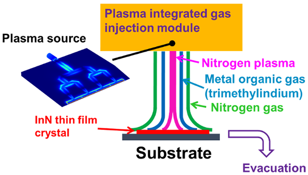
Schematic diagram of a source gas injection module that integrates a plasma source and an indium source gas supply line
Indium nitride (InN) has the highest electron mobility among nitride semiconductors of 14,000 cm2/Vs (theoretical value), and has a bandgap energy (0.7 eV) corresponding to near-infrared (1.8 μm). As such, it holds promise as base material for next-generation high-frequency devices for post-5G and for near-infrared optical devices such as lasers that have low temperature dependence of wavelength.
The emission wavelength of indium gallium nitride (InGaN) semiconductors can be increased from ultraviolet to near-infrared by increasing the In content. So applications such as high-efficiency solar cells that cover the wavelength range of ground-level sunlight and micro-light-emitting-diode (micro-LED) that emit red light are also attracting attention. However, the realization is thought to require InGaN with In content of 30 to 100 % (100 % is InN) and 30 to 40 %, respectively.
When using the metal organic chemical vapor deposition (hereafter “MOCVD”) method to grow InN and high In-content InGaN, it is extremely important to control the growth temperature. In atoms easily desorb from the growth surface and are rarely incorporated into the crystal at temperatures of 800 °C or more, so growth must be performed at a low temperature of 650 °C or less. However, the conventional MOCVD method uses thermal decomposition of ammonia gas, so a high temperature of 900 °C or more is needed to efficiently decompose the ammonia gas. At the low temperature of around 650 °C needed for growth of InN and high In-content InGaN, a sufficient amount of reactive nitrogen species cannot be supplied to the growth surface, making it a challenge to create thin-film crystals with the high electron mobility and high emission efficiency demanded by high-performance devices.
Researchers in AIST developed a new vapor deposition technology for thin-film crystals for nitride semiconductors and in particular indium nitride (InN) and high In-content indium gallium nitride (InGaN).
This technology integrates an original quasi-atmospheric pressure plasma source into the source gas injection module of a conventional MOCVD system, enabling to successfully enhance the quality of InN thin-film crystals by supplying high-density reactive nitrogen species to the sample surface. This achievement is expected to realize high-efficiency optical devices in the red to near-infrared range required for applications such as next-generation solar power generation and VR/AR displays, and next-generation high-frequency devices.