Yuki Noda (AIST Postdoctoral Researcher), Sachio Horiuchi (Leader), Tatsuo Hasegawa (Principal Research Manager) and others of the Flexible Materials Base Team, the Flexible Electronics Research Center (Director: Toshihide Kamata) of the National Institute of Advanced Industrial Science and Technology (AIST; President: Ryoji Chubachi), in collaboration with Fumitaka Kagawa (Unit Leader) of Dynamic Emergent Phenomena Research Unit, the Center for Emergent Matter Science, RIKEN (President: Hiroshi Matsumoto), Reiji Kumai (Professor) of Condensed Matter Research Center, the Institute of Materials Structure Science, the High Energy Accelerator Research Organization (KEK; President: Masanori Yamauchi), have developed a fabrication technique for single-crystalline thin-film arrays of an organic ferroelectric small molecules working as a memory device by using a solution process under ambient pressure at room temperature.
For fabrication of organic ferroelectric devices, one of the problems to be solved is to make a homogeneous thin film. The developed printing technique that stimulates thin-film formation from a solution allows formation of highly uniform single-crystalline thin films of organic ferroelectrics. The thin-film device fabricated by the developed technique worked as a memory device with only 3 V which is lower than operation voltage of various memory devices. The developed technique is expected to accelerate the research and development on low power consumption device of printed electronics such as ferroelectric memories and nonvolatile semiconductor FETs.
Details of the results will soon be published online in a German scientific journal, Advanced Materials.
 |
|
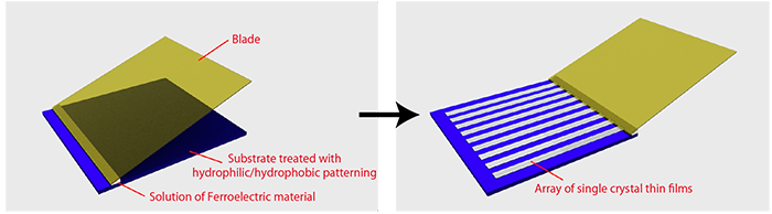
Schematic of fabrication process of single-crystalline thin films of organic ferroelectric molecules |
Active R&D of the "printed electronics", which applies printing technologies to the production of electronic devices by forming precise, high-quality, metallic and/or semiconducting patterns, has been conducted globally. So far, several printing methods have been enthusiastically developed to fabricate metallic wires and semiconductor layers for transistors, although the development of printing techniques for other types of materials has not been conducted enough. Ferroelectric materials could reduce the power consumption of electronic devices such as ferroelectric memories in IC cards and nonvolatile semiconductor FETs. Therefore, it is required to develop patterning techniques for ferroelectric thin films though printing technologies.
Ferroelectric materials are generally composed of inorganic materials so that it was considered to be difficult to apply a printing process. Although organic ferroelectric polymer materials are applicable to a printing process, their ferroelectric characteristics are inferior to those of inorganic materials. In recent years, research and development of organic ferroelectrics composed of small molecules have advanced. Some new organic materials showing superior characteristics comparable to inorganic ones have been found. Though thin-film formation of these materials is indispensable for making them into devices, it is difficult to form thin films of the materials. Therefore, it was desired to develop a fabrication technique of uniform thin film without any pinholes through a printing process.
AIST has been promoting the research and development of organic ferroelectric small molecules composed of light elements, which contain no rare metal nor toxic lead and could be suitable for print production technologies. It has developed many organic ferroelectrics, including a binary component molecular compound with excellent ferroelectric properties (AIST press release on January 24, 2005) and a single component material that exhibits the best ferroelectric properties at room temperature (AIST press release on February 12, 2010). To build them into devices, it is necessary to fabricate pinhole-free, uniform thin films with oriented molecules. These demands motivated the researchers to search an appropriate compound and to adopt an advanced printing technique.
This study is supported by the Japan Science and Technology Agency through CREST, as “Creation of Materials Science for Advanced Ferroelectrics of Organic Compounds.” (Research Period: FY2011 - FY2015)
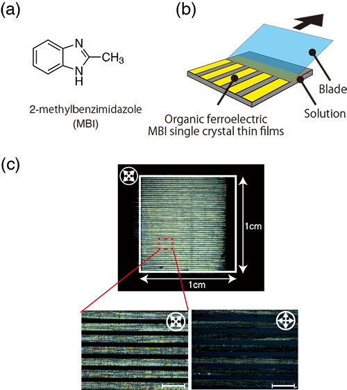
The researchers selected 2-methylbenzimidazole (MBI) as a promising candidate for an organic ferroelectric material (Fig. 1a). MBI is one of the hydrogen-bonded organic ferroelectric materials, is soluble in organic solvents, shows polarization reversal at a low coercive electric field (few tens kV/cm), and exhibits excellent ferroelectric properties at room temperature. Within a single crystal, remnant polarization P would appear in two orthogonal directions. In devices to which voltage is applied in a direction normal to the thin film, P should have a component normal to the thin film. MBI is expected to grow in plate-like crystals having a desired polarization direction.
Figure 1b shows the schematics of the developed thin film print fabrication process under ambient pressure at room temperature. First, the surface of a 1 cm square SiO2/Si substrate was treated with hydrophilic/hydrophobic patterning consisting of a 100 µm line and space (L&S) structure. An array of crystalline thin films can be formed on the hydrophilic regions by shearing the solution of MBI with a flat blade and successive drying. Synchronized light extinction by rotating cross-polarizers in the crossed-Nicols optical micrographs indicated a high degree of crystallographic alignment of these thin plate-like crystals (Fig. 1c).
 |
|
Figure 1: (a) Molecular structure of MBI. (b) Schematics of fabrication method for single-crystalline thin film. (c) Crossed-Nicols polarized micrographs of MBI thin films. Rotation of the sample (or rotation of the polarizers) changed the brightness. Crossed arrows indicate the directions of the polarizers. Scale bars: 400 µm. |
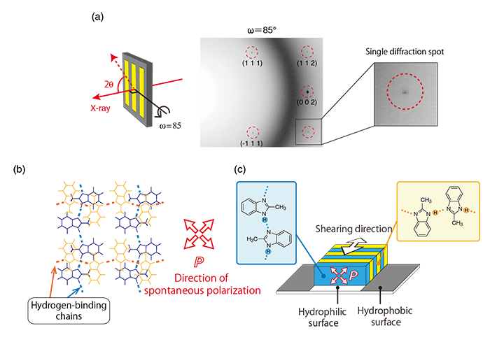
The lattice parameters, crystal orientations, and directions of spontaneous polarization of the MBI film were determined by synchrotron X-ray diffraction measurements at the Photon Factory of KEK. A single diffraction spot (in the dashed red circle) was observed for each diffraction plane (Fig. 2a) suggesting the formation of a single crystal. Figures 2b and 2c show schematics of the molecular packing structure and crystal orientation on the substrate. It was found that one of the hydrogen-bonded chains is directed perpendicular to and another is parallel to the substrate surface, respectively. It means that the principal polarization axes are tilted by 45 degrees relative to the substrate surface. As the spontaneous polarization has a component perpendicular to the substrate, it may be possible to reverse the polarization in electrode/ferroelectric/electrode layered structure by applying voltage between upper and lower electrodes.
 |
|
Figure 2: (a) Schematic of synchrotron X-ray diffraction experiment and diffraction pattern of plate-like crystal, (b) Molecular packing structure within crystals, (c) Schematic of molecular chain and polarization alignment on substrate surface. |
A capacitor-type device using the plate-like crystals with about 1 μm thickness exhibited quasi-rectangular loops in the electric polarization (P) versus electric field (E) hysteresis experiments without additional thermal annealing (Fig. 3a). The devices exhibited polarization switching at a very low voltage of about 3–4 V at 10 Hz. The fatigue characteristics of switching were evaluated at frequencies of 10, 100, and 1000 Hz. The ferroelectric properties could be maintained until hundreds of thousands cycles at 1000 Hz (Fig. 3b). The researchers expected that the fatigue characteristics could be improved by optimizing the device structure.
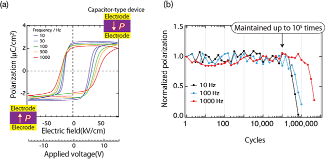 |
Figure 3: Ferroelectric properties of the developed single-crystalline thin film
(a) Electric polarization (P) versus electric field (E) hysteresis loops. (b) Fatigue characteristics at frequencies of 10, 100, and 1000 Hz |
Piezoresponse force microscope (PFM) characterization provides microscopic information about the polarization reversal. Figure 4a shows various sizes of polarization reversal domains obtained by applying a constant DC bias of +20 V to the tip with a pulse duration varying from 10 to 1000 ms for a 1.0 µm thick film. The minimum domain size was ≈500 nm, whereas it increases logarithmically with increasing a pulse duration (Fig. 4b). This domain was found to be stable for at least 40 h under ambient pressure at room temperature. Phases of PFM images reveal that the polarization changes by not 90 degrees but 180 degrees (Fig. 4c).
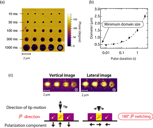 |
Figure 4: Local polarization reversal by using a piezoresponse force microscope (PFM)
(a) PFM phase image of written domains. (b) Size variation of polarization reversal domains as a function of pulse duration for an applied electric field. (c) Phase images of vertical and lateral directions |
The researchers aim to develop manufacturing technologies of all-printed electronics devices by combining the developed printing technique for thin film formation and other printing techniques for fabricating metal wires and semiconductor thin films.