-Development of a platform for performance evaluation at the memory array level –
Hiroyuki Akinaga (Deputy Director), the Nanodevice Innovation Research Center (Director: Toshihiko Kanayama) of the National Institute of Advanced Industrial Science and Technology (AIST; President: Tamotsu Nomakuchi), and Hisashi Shima (Research Scientist), Superior Nano-interface Device Research Team of the center, have developed a process for integrating low-power, high-speed, and non-volatile resistance random access memory (RRAM) devices on a 128-kbit memory chip and have succeeded in fabricating chip arrays on an 8-inch wafer. This research has been performed in collaboration with Sharp Corporation (Sharp; President: Mikio Katayama), the Institute of Semiconductor & Electronics Technologies (Director: Suu Koukou) of ULVAC, Inc. (ULVAC; President and CEO: Hidenori Suwa), and Akio Kitagawa (Associate Professor) and Kazuya Nakayama (Associate Professor) of the Graduate School of Natural Science and Technology (Dean: Yoshihiro Fukumori), Kanazawa University (President: Shin-ichi Nakamura).
This RRAM chip array was fabricated by using the existing semiconductor manufacturing process and uses neither expensive components such as noble metal electrodes nor materials requiring special handling. Because of this, it is a memory device that is bit-cost competitive and saves natural resources and energy.
RRAM is the key to energy efficiency in the areas of information and electronics, in which the use of devices with the ability to handle large amounts of information at high speed is becoming increasingly important. Our research has led to the development of a platform for evaluating the performance and reliability of RRAM devices at the chip and wafer levels. Our next goal is the early application and commercialization of this new memory device.
This achievement will be presented on May 18 at the 2nd International Memory Workshop in Seoul, Korea, from May 16 to 19, 2010.
 |
|
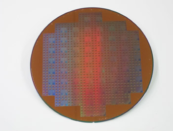
Photo 1 A 128-kbit RRAM chip array fabricated on an 8-inch wafer |
In recent years, as society has become increasingly information-oriented, IT equipment such as a PC has become essential for industrial activities and daily life and has become widely used. Consequently, power consumption by IT equipment is rapidly increasing and accounts for a significant proportion of Japan's total power consumption. Although the performance of IT equipment has continued to be improved, the required capacity of memory devices has kept increasing as the functionality of equipment has been continuously sophisticated. Reducing the power consumption of memory devices is considered to be an effective way of improving the energy efficiency of IT equipment. In other words, there is a demand for low-power memory devices that can operate as fast as, or faster than, current mainstream dynamic RAM (DRAM); there is a particular demand for non-volatile memory devices that require power only to read and write data but not to retain data.
RRAM is a memory device in which a transition metal oxide film is sandwiched between a pair of metal electrodes and the change in the electrical resistance of the oxide film is used as memory information. Because of its low power consumption and short rewrite time, RRAM is a promising candidate for a next-generation non-volatile memory device to support an advanced information-based society, and the realization of practical RRAM is expected.
AIST has investigated the phenomenon of resistive switching and has conducted research on its application. It has also been conducting RRAM research and development based on this phenomenon. In 2006, we succeeded in increasing the operating speed of an RRAM device. Subsequently, we conducted research and development to achieve low-current and high-speed operation and to quantitatively control the operation of RRAM. In 2008, we developed a very-low-power, high-rewrite-speed RRAM device.
As a result, the performance of the device itself has improved dramatically. However, for practical application of the device we need to solve the problems associated with the integration of memory devices, guarantee the overall performance of the integrated memory device based on the statistical reliability data, and develop a mass-production process technology for the memory devices at the wafer level. To this end, we decided to develop a process for fabricating an integrated circuit and a memory array at the wafer level, as well as an evaluation platform for testing the reliability of a memory array.
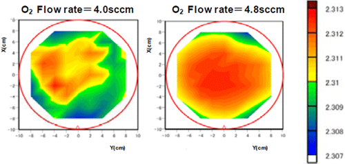
Most non-volatile memory devices that are candidate post-flash memory devices use special materials that are not used in existing Si production lines and therefore require the development of peripheral elemental technologies and additional capital investment. Despite the superiority of these non-volatile memory devices to flash memory in terms of performance, the fact that their development has not been able to catch up with the speed of miniaturization of flash memory has formed a significant barrier to their practical application. Sharp and ULVAC have developed film forming and processing technologies for the uniform and reliable fabrication of RRAM device structures on an 8-inch wafer, which was developed in 2008 and allows very-low-current and high-speed operation, and they have integrated the device structures into a 128-kbit memory chip. Photo 1 shows the developed RRAM chip array. Approximately 100 RRAM chips are formed on an 8-inch wafer. Materials commonly used in the current complementary metal-oxide-semiconductor (CMOS) process are used in the RRAM memory device. This provides good affinity between the RRAM devices and CMOS processes, making it possible to integrate RRAM chip arrays by using existing semiconductor microfabrication technology. This allows minimization of additional capital investment, making RRAM devices bit-cost-competitive memory devices. In order to evaluate the uniformity of quality of oxide film, an important factor in fabricating a memory array on an 8-inch wafer, the refractive index of the thin film on the wafer was measured (Photo 2). The different colors in the photo indicate different refractive indexes, representing the difference in film quality. A uniform thin film was formed on the 8-inch wafer by controlling the amount of oxygen used to form the film (Photo 2, right).
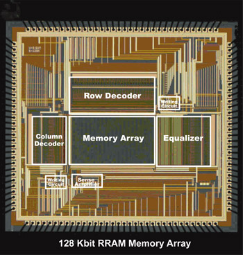
Photo 3 is an enlarged view of the RRAM memory array chip. The chip is about 5 mm square. In addition to the memory array formed on the chip, address decoders, an equalizer, a sense amplifier, and a write circuit are mounted on the chip. Data are written using the address decoders and the write circuit, and read by the sense amplifier.
This RRAM memory array chip has an evaluation circuit designed by Kanazawa University, allowing evaluation of the reliability of a memory array. Sixteen different test element groups with a memory array of 2 to 128 kbits are formed on the chip. Transistors incorporated into the chip are used to control the operating current of the memory array, allowing evaluation of the reliability of a 1T-1R (1 transistor-1 RRAM) structure. If a memory device can be operated at a low current, these transistors can be miniaturized, enabling the mass production of chips and increasing the capacity of the memory array.
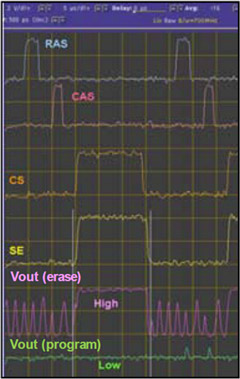
Photo 4 is an example of the sensing operation of the 128-kbit RRAM memory array that was developed. The memory array contains a number of integrated memory devices. In Photo 4 the location (address) for writing or reading data is specified by three control signals: Raw Address Strobe (RAS), Column Address Strobe (CAS), and Chip Select (CS). Subsequently, the data stored in the specified address is output to Vout by converting the variation in resistance stored in the RRAM device to a variation in voltage: this conversion is controlled by the Sense Enable (SE) signal. The two results of data read from the memory device, the state of data 1 written (erase) and the state of data 0 written (program), are superimposed in Photo 4. The time required to read data is only 8.5 ns. This circuit makes it possible to check the operation of a memory array, develop an operation algorithm, and perform statistical reliability evaluation.
A platform for checking the operation of a memory device at the chip and wafer levels and for performing reliability evaluation has been developed. Several different memory arrays can be fabricated on a chip to provide flexibility in performing various reliability evaluations. The chip fabrication technology established at the wafer level is expected to accelerate research and development for the early application of RRAM.
 |
|
Photo 2 Dependence of the refractive index distribution in an 8-inch wafer on film-forming conditions |
 |
|
Photo 3 The 128-kbit RRAM memory array chip |
 |
|
Photo 4 Example of sensing operation of the developed memory array |
align="left">The reliability of an RRAM device will be evaluated at the array and chip levels on the evaluation platform that has been developed. Issues associated with commercialization will be identified and solved to achieve the early application and commercialization of RRAM devices.