- Successful creation of a 10A trial device for energy-saving domestic electrical appliances -
The Power Electronics Research Center (Director: Kazuo Arai) of the National Institute of Advanced Industrial Science and Technology (President: Hiroyuki Yoshikawa) (hereinafter referred to as AIST) has developed a technology for creating a device called an implantation and epitaxial MOSFET (IEMOS) on the carbon face of a silicon carbide (SiC) .
There is a considerable degree of expectation that SiC will be the material that is used in the next generation of energy-saving power devices because of to its ability to control large amounts of power. AIST had already developed an IEMOS that realized the world’s then lowest resistance of 4.3 mΩcm2, and this time we achieved an even smaller resistance of 1.8 mΩcm2 by creating an IEMOS on the carbon surface of a SiC crystal. Because this is about one-tenth or less of the resistance of Si power devices in current use, the new device shows a power loss of about one-tenth of that of a conventional Si power device.
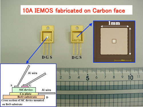
We also created a device of with the capacity to carry currents of the 10A level, as required for use in domestic electrical appliances (Figure 1). This device is expected to decrease the power consumption of appliances such as induction heaters, air-conditioners, and PC servers.
The results of the research were scheduled to be presented in detail at the 2006 International Electron Device Meeting (IEDM), held on December 11th and 13th, 2006 in San Francisco.
 |
|
Fig. 1 10A level SiC device using IEMOS on carbon face. |
The silicon (Si) semiconductors that are used in PCs are inadequate for controlling large amounts of power, but are widely used in products such as diode rectifiers and inverter controllers despite this inadequacy. If silicon carbide (SiC) semiconductors, which have excellent characteristics, could be used to replace Si semiconductors, it would be possible to control much more electrical power with a smaller power loss.
Theoretically, the resistances (on-resistance) of SiC devices are two orders of magnitude lower than those of comparable Si devices when a current is applied. Power losses would be expected to decrease considerably should SiC be used in domestic electronic appliances such as induction heaters, air-conditioners, or PC servers, in semiconductor devices for automobiles, or for electric transmission and distribution system. If practical application of SiC devices were to accelerate the introduction of inverters for power-electronics products, as much as 4,466 kL of crude oil could be saved annually by 2030.
SiC substrates are already being marketed by Japanese, European, and American companies. 4 inches substrates are already available on the market An industry market based on SiC devices are increasing. The practical application of SiC device is accelerating, as European and American companies have started to sell SBDs.
The SiC power MOSFET, a switching device that has a small resistance in the operating mode (the on-resistance) and a fast switching speed, is highly promising, but its on-resistance is far larger than the theoretical limit, although it is still smaller than that of Si. It cannot therefore perform to its maximum when used in an air conditioner or induction heater.
The SiC power MOSFET is generally created in a structure called a double-implanted MOSFET (DIMOS). The SiC region called the P well that is adjacent to the gate oxide film is created by heat treatment at temperatures above 1,600 ºC following doping by aluminum ions (Figure 2 and 3). During this process, Si evaporates from the SiC surface, which is smooth before the heat treatment, and the surface becomes rough and irregularities grow in size (Figure 3). Electrons flowing on the surface collide with these irregularities and are scattered. The channel mobility becomes smaller, and the overall resistance increases.
To overcome this situation, AIST has developed a structure called an implantation and epitaxial MOSFET (IEMOS) (Figures 4 and 5). Because the surface of the P well in the IEMOS consist of an epitaxial layer, heat treatment at above 1,600ºC is not required and the surface remains smooth (Figure 5). Accordingly, the flow of electrons improves and the channel mobility increases, reducing the overall resistance. These developments combine to make a device with the smallest ever resistance of 4.3mΩcm2 a reality.
AIST has been developing this device supported by New Energy and Industrial Technology Development Organization (NEDO) via the Ministry of Economy, Trade and Industry. The basic technology of the SiC device was developed as a part of the “Development of electronic devices with a very low power loss” project (from 1998 to 2002), and the SiC device was developed as part of the “Strategic development of technology for rational energy usage” project (from 2003 to 2005). This research work is being conducted as a part of the NEDO project “A fundamental technology development for power electronics inverter”, which began in July 2006
This announcement relates to the development by AIST of a technology for creating an IEMOS on the carbon surface of a SiC crystal that has diverse plane directions (Figure 6). SiC devices are normally created on a silicon surface, which is a typical plane orientation. One of the reasons for this is that although a SiC device is created on a SiC epitaxial substrate formed as a concentration-controlled epitaxial layer on a SiC substrate, the epitaxial layer is created on the silicon face of the SiC crystal because until recently it was believed that it was impossible to create a P-type epitaxial layer on the carbon face. The Power Electronics Research Center has, however, now developed a technology that permits it to create a P-type epitaxial layer on the carbon surface for the first time ever.
The other achievement of the project is an improvement in the method for creating the gate oxide film. The defect density of the interface between a carbon surface and a gate oxide film is higher than that between a silicon surface and a gate oxide film. We created a gate oxide film by using vapor and with subsequent annealing in hydrogen. This method produced a lower defect density at the carbon surface than at the silicon surface and it increased the mobility of the channel domain by about 60% compared with that of the silicon surface. We thus succeeded in reducing the channel resistance considerably (Figure 7).
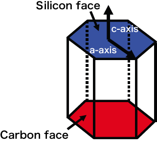
Fig. 6 Crystal structure of SiC
|
|
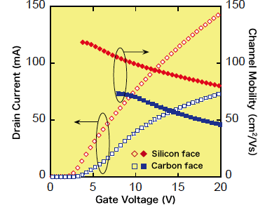
Fig. 7 Comaprison of carbon face and silicon face
|
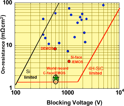
Because the channel resistance accounts for the majority of on-resistance of a switching device based on a SiC power MOSFET, the reduced channel resistance leads to a considerable decrease in on-resistance, resulting in a device with the world’s smallest ever resistance of 1.8 mΩcm2 (Figures 8 and 10).
We created a device with an area of 1 mm2 and found that it was capable of handling a current of 10 A and of withstanding a dielectric breakdown voltage of 660 V (Figure 9), allowing it to be used in domestic electrical appliances such as induction heaters, air conditioners, or PC servers. In addition, this device is of the normally-off type: no current flows when a gate voltage is not applied, allowing it to control electrical currents easily when it is used in an inverter.
At present, the smallest on-resistance of a Si power device is about 20 mΩcm2. The on-resistance of the newly developed power device is 1.8 mΩcm2, which is less than one-tenth of the on-resistance of a Si power device. It is expected that SiC power device will replace Si power device in domestic electrical appliances to assist in energy-saving efforts.
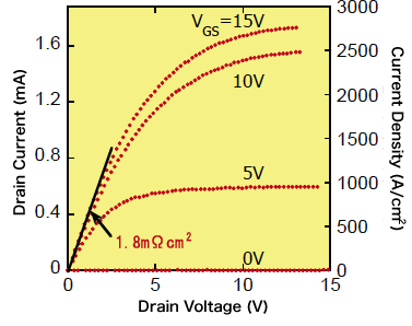
Fig. 8 I-V charactersitics of developed IEMOS
|
|
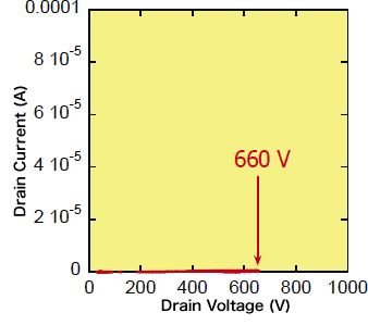
Fig. 9 Reverse charactersitics of developed IEMOS. Current does not flow up to
660V, large current flows more than it, and then devices breakdown.
|
 |
|
Fig.10 Relationship between on-resistance and blocking vlotgae. IEMOS on silicon
face has been ever reported. IEMOS on carbon face is reported in this.
|
We successfully achieved an on-resistance of less than 1.8mΩcm2 in a unipolar device that was capable of withstanding voltages as high as 660 V and we created a 10A trial device for the first time ever. We will clarify the ultimate performance of a SiC inverter utilizing such a device with a capacity more than 10 A in the NEDO project “A fundamental technology development for power electronics inverter” We wish to create an inverter for testing under realistic conditions to study its performance.
We wish to accelerate the spread and commercialization of SiC devices by establishing the applicability of such devices in domestic electrical appliances such as air conditioners and induction heaters, in automobiles, or in electric transmission and distribution system . We will also consider providing samples of SiC devices to manufacturers of power-electronics equipment.
The epitaxial growth technology has already been transferred to ESICAT Japan, LLP, a venture organization founded in 2006 by researchers from AIST, the Central Research Institute of Electric Power Industry, and Showa Denko K.K. SiC epitaxial wafers are currently available on the market.