- Acceleration of technical development for practical use, such as fabrication and repair of nano-molds -
The National Institute of Advanced Industrial Science and Technology (AIST; Hiroyuki Yoshikawa, President) and Toyama University (Tokuso Saito, President) have jointly developed a nano-mechanical fabrication system working in a scanning electron microscope (SEM), and thereby succeeded in real-time imaging of the nano-scale cutting process for a single crystal of silicon.
The fabrication system we have developed utilizes the mechanics of atomic force microscopes (AFM), in which we use a special cantilever for fabrication which has been developed by ourselves. For nano-scale cutting in this system, the cutting depth can be controlled in the range of 1-100 nm (1 nm = 10-6 m) by changing the normal load applied to the cutting edge fixed on the cantilever tip. The tip of the cutting edge can be observed by SEM, and thereby the nano-scale cutting process can be recorded as a movie.
The direct observation of the fabrication process can provide more valuable information than point signal logging, and can thus be a powerful tool for clarifying the removal mechanism of materials by cutting and for determining optimal fabrication conditions. The developed nano-fabrication system operating in SEM is expected to accelerate development of the practical use of nano-fabrication techniques, e.g. fabrication and repair of nano-molds etc. used in nano-imprints.
A cantilever used for fabrication |
|
A SEM image of the nano-cutting process (captured from movie)
|
Mechanical fabrication is the oldest and the most familiar of manufacturing technologies, and is still used for the fabrication of a wide range of materials in present-day industries. Various structures and mechanical parts are produced in a precision of micro-meter order. Mechanical fabrication is based on the basic principle of shaving off parts of a material using solid tools. Theoretically, in a fundamental-experiment level, it has been proved that nanometer-scale fabrication is possible, if a tool with an ultra- sharpened tip of nanometer orders and an ultrahigh-precision driving system were available. For several years, nano-mechanical fabrication technologies utilizing AFM mechanics have been used in practice, e.g. as repair of photo-masks for LSI, and thus as techniques applicable to nano-fabrication technologies, and expectations for nano-mechanical fabrication have been increasing. Although the principle of the mechanical fabrication seems simple, especially for small-scale fabrication, it is very difficult to observe the fabrication process directly. Thus, most of the various phenomena occurring in the fabrication process have been unclear, and machine operators have had to decide the optimal condition relying on intuition and experience rather than theory.
We have been studying nano-scale cutting fabrication with AFM mechanics for ten years, and have carried out basic experiments enabling the observation of cutting behaviors by uniquely developing a nano-scale cutting system and a cantilever for cutting fabrication, a key device in this system.
Also, we have studied the accuracy of fabrication which is one of the most very important factor for fabrication technologies, and the development of sharpening techniques for the cutting edges of fabrication cantilevers, and carried out the development of a 3-dimensional nano-fabrication and measuring system in the "Regional New Consortium Projects",which is supported by government, METI., Direct observation of the nano-cutting process is essential to understand fabrication mechanism or phenomenon. From this viewpoint, we have carried out this research work under the support of the "Industrial technology Research Grant Program in '03 and '04" of the New Energy and Industrial Technology Development Organization (NEDO).
 |
|
Figure 1 Fundamental experiment procedure for nano-cutting fabrication |
In this work, there are two major factors to develop; one is the design and construction of a nano-fabrication system operating inside the SEM, and the other is the development of the fabrication cantilevers.
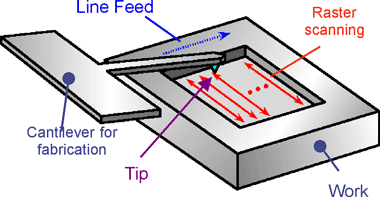
Figure 1 shows a schema of the experimental procedure of nano-mechanical fabrication with AFM mechanics. By indenting a cutting edge fixed on the cantilever tip against the material surface and then raster scanning relatively between the cutting edge and the surface, the material of a square region of the surface can be removed. To observe the nano-cutting process, a view angle from the diagonal direction to the front of the cantilever must be maintained.
Figure 2 shows a special SEM stage integrating a nano-fabrication system. These are uniquely designed to avoid interference with the SEM lens system and to preserve an observation angle. The system has to be installed in a vacuum chamber, so a non-resonant ultrasonic actuator is applied to reduce the mechanical drive system.
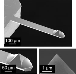
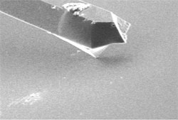
Figure 3 shows a cantilever for fabrication with a sharpened tip made of CVD diamond. This tip is formed by using a pyramidal silicon mold which is fabricated by anisotropic etching. Until now, as a cutting edge, single diamond abrasive grain has been used, fixed on the cantilever tip. However, the irregularity of the grain shape causes unevenness in fabrication performance, and thereby it was quite difficult to identify the cutting points . The sharpened cutting edges we have formed have a geometrically regular shape with a tip apex of 30 nm in radius, resulting in a good cutting performance.
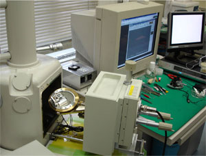
Figure 2 A nano-fabrication unit integrated in SEM stage |
|
Figure 3 A cantilever for fabrication with a sharpened tip
|
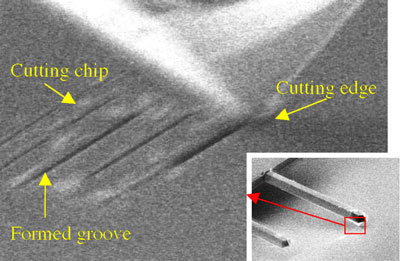
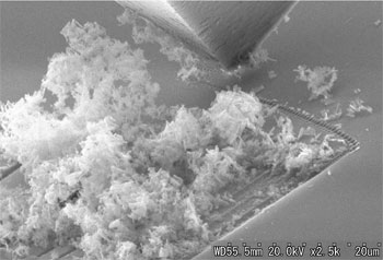
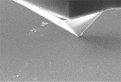
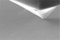
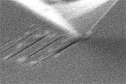
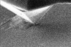
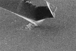
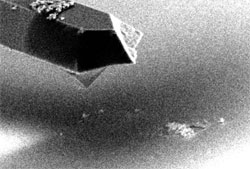
Figure 4 shows a SEM image of a cantilever cutting edge after nano-cutting experiment and the periphery. By the cutting, the material surface is partially removed, and many cutting chips are left on the surface. Figure 5 shows still images captured from movie recorded in the nano-cutting process. Several grooves, shown in Figure 5(e), are formed by fabricating toward right with stepwise increasing normal-load applied to the cutting edge; it is clearly seen that the depth of the grooves increases gradually. The cutting action is done at the edge toward the front of the cantilever (visible edge side in pictures). The cutting depth can be estimated to be approximately 100 nm from the pitch of the line feed of scanning.
 |
|
Figure 4 A SEM image of a cutting edge tip and the periphery after nano-cutting |
The single crystal silicon used is a comparatively hard material, usually referred to as one of the "brittle" materials. In macro-scale mechanical fabrication, it behaves as a fragile material like glass. However, our experimental results demonstrate that, in nano-cutting fabrication, the ductile-mode cutting is performed even for brittle materials as well as the usual metallic materials. Thus, we have experimentally confirmed that the nano-mechanical fabrication is applicable to a variety of materials, such as metal and glass, because single crystal silicon is harder than the usual metallic materials.
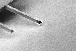
(a) A whole cantilever before cutting
|
|
(b) A cantilever tip before cutting
|
(c) A cutting edge of tip before cutting
|
|
(d) After three-step loading in the cutting process
|
(e) After five-step loading in the cutting process
|
|
(f) Generating cutting chip during cutting
|
(g) Immediately after cutting
|
|
(h) After lift out
|
|
Figure 5 SEM images showing the status of the nano-scale cutting process |