- Enabling the realization of 50 nm fabrication over a wide area at high speed and low cost -
The National Institute of Advanced Industrial Science and Technology (AIST; Dr. Hiroyuki Yoshikawa, President) has succeeded in the development of a nano-fabrication technique utilizing a thermal lithography method resulting from the combination of visible-light lithography using a semi-conductor laser with a thermally nonlinear material. By combining the thermal lithography technique of AIST with optical disc-related techniques of Pulstec Industrial Co. Ltd. (Tatsuo Kinoshita, CEO), a nano-fabrication apparatus has been developed.
The apparatus we have developed enables the formation of 50 nm-fine structures over a wide area of 12 cm in diameter, the size of an optical disc, at high-speed. It is easy to handle because of its desktop size, and its price is one fourth of the corresponding conventional ones.
The apparatus we have developed is easily handled by anyone, and enables nanometer-scale fabrication at low cost, which until now could only be done with expensive large apparatus using short wavelength light, such as vacuum ultraviolet light (for the photolithography method) and electron beams (for the electron beam lithography method). Our technique is expected to facilitate reduction in the cost of optical devices with fine structures, e.g., photonic crystals and antireflective structures, and to be applied to nanotechnologies.
This work will be presented at the 53rd Spring Meeting, 2006 The Japan Society of Applied Physics on March 22-26 at Musashi Institute of Technology, and our apparatus will be displayed in the exhibition hall at the meeting.
Recently, the development of new devices utilizing phenomena characteristic of nanometer-scale structures has been actively carried out. For example, there have been various applications, such as antireflective nanostructures enabling a reduction in light reflection by forming nanometer-size structures smaller than the wavelength of light, photonic crystals enabling artificial control of the direction of travel of light, and 1/4 wavelength plates which can be formed as nano-structures on the surface of other optical parts.
For the antireflection structures, the reflection rate of light can be reduced over a wide angle and a wide wavelength band, and thus their application to high-efficiency solar batteries and high-brightness displays has been desired. Techniques for drawing fine patterns, called lithography, are essential to fabricate nano-structural devices. Until now, short wavelength light has been used, e.g., vacuum ultraviolet light for photolithography, and electron beams for electron-beam lithography. However, for photolithography, the development of short-wavelength light sources is becoming more difficult every year, and their development cost, including peripheral technologies for the light sources, is becoming huge. On the other hand, electron beam lithography enables 10 nm-scale drawing, but a vacuum atmosphere is needed. In addition, the drawing speed is very low, and thus this method is not used in practice for large area drawing. Furthermore, the apparatus for these methods is large and very expensive, leading to a rise in the product price. Thus, nano-lithography techniques, being inexpensive and easy for anyone to handle, have been desired.
The AIST has researched and developed high-density optical discs for the next generation after Blu-ray, and HD-DVD technologies. To highly densify recorded data, 40 nm-size recording pits are necessary, and thus AIST has developed a nano-fabrication technique for the minute recording pits, and a technique for high-speed recording on discs of 12 cm in diameter. In this work, AIST and Pulstec Industrial Co. Ltd. have jointly developed nano-structural optical devices enabling high-speed, wide-area recording and cost reduction, and furthermore developed an apparatus for easily fabricating the optical devices.
This research has been carried out in support with the "Seed growth research (fiscal year 2005)" project sponsored by the Japan Science and Technology Agency.
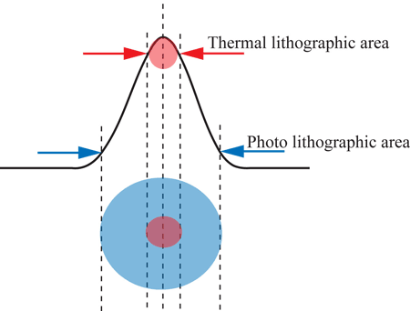
The thermal lithography method, combining visible-light laser lithography with thermal-nonlinear materials, utilizes a temperature distribution induced within the laser-light spot. Generally, for light-absorbing substances, absorbed light is transferred into heat. The intensity distribution of light focused on substrates is Gaussian, and thus when light-pyrogenic substances are irradiated by light, the induced thermal distributions may also be Gaussian (Fig. 1).
Thus, using materials which can undergo a physical change due to light-induced heat, nano-lithography with dots smaller than the diameter of the focused-light spot is made possible. In conventional lithography methods, a volume change is generated in minute regions of photoresists by a thermo-chemical reaction and thermal diffusion to draw patterns. However, for the conventional lithography methods, the fabrication of structures with a resolution of 100 or less nm and high-aspect ratios is difficult, and the reproducibility of the structures is not good. In this work, using a new material, we have developed a thermo-lithography method enabling highly reproducible formation of nano-structures less than 100 nm with high-aspect ratios, and thereby accomplished a desktop nano-fabrication apparatus (Figure 2).
 |
|
Figure 1 Drawing areas by a light-intensity distribution and thermal distribution in a focused light spot. |
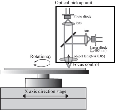
Figure 2 (a) A schematic illustration of the nano-fabrication apparatus we have developed. |
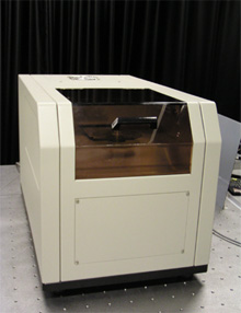
(b) An overview photo image of the nano-fabrication apparatus
|
As shown in Figure 2, the nano-fabrication apparatus we have developed in this work consists of a rotational stage, a uni-axial stage, and an auto-focus unit, enabling nanometer-scale, high-speed lithography. Also, we use semi-conductor laser beams with a wavelength of 405 nm for drawing and an optical system with an objective lens of a numerical aperture (NA) of 0.85 for focusing the laser beams, leading to the successful production of a desktop nano-fabrication apparatus, easy to handle because of its installation area of approximately 1 m2 (Figure 2(b)).
Conventional apparatus using electron-beam lithography and ArF photolithography methods can also make nanometer-scale fabrication. However, these conventional apparatuses need an installation area of, at least, 2 m2, and in addition their maintenance is very difficult, while our desktop nano-fabrication apparatus can be easily handled anywhere by anyone.
Figure 3 shows a nano-dot pattern drawn by the apparatus we have developed. The pattern was formed by rotating the disc stage at a rate of 6 m/s (2600-3600 rpm) and irradiating a blue pulse laser light. By driving a laser with a pulse frequency of 60 MHz, our apparatus can create dots of 50 nm in diameter, less than one sixth the beam spot size, at a rate of 106 dots/sec. The drawing rate for the conventional lithography apparatus, e.g., with electron-beams, is approximately 0.2 m/sec, thus indicating that our apparatus is capable of forming nano-structures at a speed of 30 times the conventional drawing rate. Furthermore, by combining our technique with a dry etching method used in the semi-conductor production process, shown in Figure 4, a nano-hole structure of 100 nm in diameter and 500 or more nm in depth can be formed over all the surface of a substrate of 12 cm in diameter (the optical disc size). Consequently, using the nano-fabrication apparatus we have developed, molds with nanometer-scale fine patterns for nano-imprint can be fabricated over a wide area at high speed and low cost.
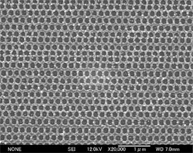
Figure 3 |
|
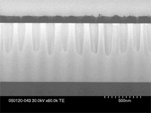
Figure 4
|
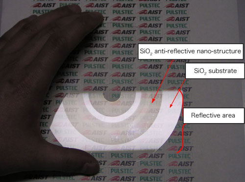
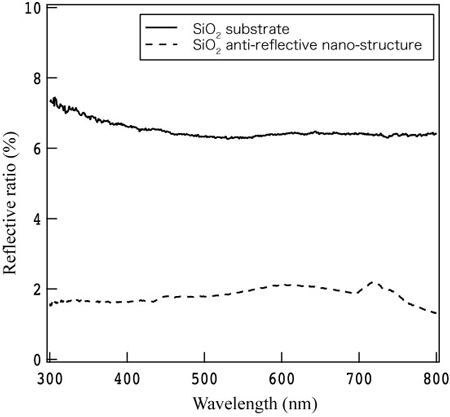
Figure 5 also shows that the reflection rate of light can be reduced by forming an antireflective nano-structure on the surface of a SiO2 disc of 12 cm in diameter; a part of the flat SiO2 substrate looks white due to the reflection of fluorescent tube light, while, in the part with an antireflective nano-structure, the letters AIST and PULSTEC at the back of the disc are clearly visible due to reduction in the reflected light. Thus, by inexpensively producing antireflective nano-structures over a wide area at high-speed, we can also give the antireflection performance to displays and lenses of digital cameras at low cost, which Japan excels in, enabling a significant contribution to a product development field in which global competition is increasing.
 |
|
Figure 5 A photo image of an antireflective nano-structure formed on a SiO2 disc substrate of 12 cm in diameter and refection rate characteristic for the part with or without the nano-structure. |