- Flexible micro-fabrication on silica glass through progressive photochemical processing induced by UV laser irradiation on centimeter-sized area: etching a micro-trench with a maximum aspect ratio of 60 -
The National Institute of Advanced Industrial Science and Technology (AIST), an independent administrative institution, (president: Prof. Hiroyuki Yoshikawa) has developed two manufacturing equipments for flexible micro-fabrication of silica glass having a deep trench structured by novel laser-induced photochemical processing on centimeter-sized area of glass.
The high precision surface microfabrication of the UV-transparent materials such as a silica glass is one of the key technologies of photonics research and development. Processing of large surface area of the materials is required for industrial application. However, silica glass is a hard and brittle material, and precision surface microfabrication is very difficult.
The new equipments based on AIST-original technology of "Laser-induced backside wet etching (LIBWE)" consists of excimer laser mask projection system and DPSS (diode-pumped solid state) laser beam scanning system. In the LIBWE technique, protection layer, that is indispensable in conventional lithography processing, is unnecessary on the material surface. The two new systems allow us to use rapid prototyping of high precision surface microfabrication of silica glass (Fig.1). The research group is going to develop a silica glass microdevice for photonics applications.
 |
|
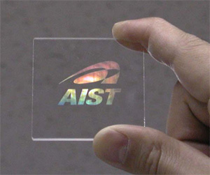
Fig.1 Line patterned grating fabricated by laser beam scanning system using galvano mirrors. (Color image on silica glass is obtained by visible light scattering with the grating) |
UV-transparent materials such as a silica glass are widely used for optical devices practically. The precision surface microfabrication of the materials to make highly integrated microdevices is one of the key technologies of photonics research and development. For practical processing, surface microstructures on silica glass are fabricated by conventional etching techniques with reactive plasma gas or hydrogen fluoride (HF) solution. As the conventional techniques consist of complicated multi-step processing of (i) protection layer coating (photoresist), (ii) lithography, (iii) etching, and (iv) cleaning, a new technique would be required to reduce the steps.
Since 1999, the research team of Laser-Induced Materials Processing Group in Photonics Research Institute (PRI), AIST has investigated UV laser-induced surface microfabrication of silica glass by using their own original technique in terms of novel laser-induced photochemical processing that was named as LIBWE. The idea of LIBWE is based on the deposition of laser energy on the surface of silica glass during the laser ablation of a dye solution with a nanosecond-pulsed UV laser. Improving laser irradiation optical system and optimizing dye solution composition promoted the surface micro-fabrication property and optical characteristic of silica glass. LIBWE technique is a kind of indirect excitation processing by laser irradiation. LIBWE technique has attracted attention from the community of laser materials processing research, so that various overseas research institutions also investigate microfabrication of the materials by LIBWE technique. The research group in the PRI-AIST succeeded in flexible micro-fabrication having a deep trench structured by advanced LIBWE technique on centimeter-sized area.
This study was supported in part by Industrial Technology Research Grant Program in '04 from the New Energy and Industrial Technology Development Organization (NEDO) of Japan, and by "Photoreaction Control and Photofunctional Materials" project in Center of Excellence (COE) Development Program from Ministry of Education, Culture, Sports, Science and Technology of Japan.
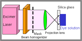
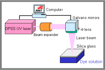
Laser-induced backsidewet etching (LIBWE) is a one-step method to microfabricate a silica glass plate through irradiation with a ns-pulsed UV laser. The concept of the excimer laser mask projection system is illustrated in Fig. 2a, and that of the DPSS (diode-pumped solid state) UV laser beam scanning system using galvano mirrors in Fig. 2b.
 |
|
Fig.2a Schematic diagram of excimer laser mask projection system. |
 |
|
Fig.2b Schematic diagram of DPSS (diode-pumped solid state) UV laser beam scanning system using galvano mirrors. |
The LIBWE method is a resist-less, single-step surface microstructuring process. These characteristics provide great advantages compared to HF etching or plasma etching, both of which require complicated sequences for patterning a photoresist involving photolithography or electron beam lithography as a pre-treatment, etching, and the removal of the photoresist by solvents as a post-treatment.
By using a mask projection system, the research team has succeeded in the micro-fabrication of silica glass up to 1 micron resolution as a minimum resolution, and a deep micro-trench about 7 microns wide and 420 microns deep with a maximum aspect ratio of 60 (Fig.3). The micro-trench was successfully fabricated by the irradiation of 25,000 pulses at 80 Hz, giving a processing time of about 5 minutes. The etch rate was calculated to be approximately 17 nm pulse-1 at 80 Hz, or 1.3 micron sec-1, which is two orders of magnitude larger than that for HF etching or plasma etching.
By using DPSS (diode-pumped solid state) laser beam scanning system with the galvanometer according to the pattern produced on a computer, a centimeter-sized component structured by a line-patterned grating was easily fabricated on a silica glass plate upto 5 x 5 cm2 area. Figure 1 shows a line patterned grating of "AIST-logo" on silica glass fabricated by the laser beam scanning system. Color image on silica glass is obtained by visible light scattering with the grating. It is demonstrated that galvanometer-based point scanning system is suitable for a flexible rapid prototyping without a mask projection.
Well-defined microfabrications of various transparent materials, such as silica glass, quartz, glasses (Pyrex, etc.), calcium fluoride, magnesium fluoride, barium fluoride, fluorocarbon resin, and sapphire, have been investigated.
The research group is going to develop microdevices and imprinting template of surface-structured silica glass for photonics applications.
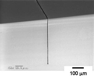
Fig.3 Cross-sectional micrograph of deep trench structure (fabricated by excimer laser mask projection system).
|
|
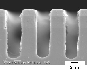
Fig.4 Cross-sectional micrograph of grating structure (fabricated by excimer laser mask projection system).
|