- Cost Reduction for Development of Semiconductor Manufacturing Process through Application of Genetic Algorithm -
Dr. Masahiro Murakawa, a researcher and his colleagues of the Advanced Semiconductor Research Center (ASRC), of the National Institute of Advanced Industrial Science and Technology (AIST), an independent administrative institution, have successfully developed high accuracy automatic fitting technology using the genetic algorithm for the next generation transistor model HiSIM (Hiroshima University-STARC IGFET Model) to be used for circuit simulation in the development of advanced semiconductor manufacturing process, in collaboration with the Advanced Materials Science Institute (Professor Michiko Miura), Graduate School, Hiroshima University (to be designated as Hiroshima University), a national university corporate.
A transistor model refers to a model to be used for the prediction of transistor circuit characteristics in the circuit simulation, and it constitutes the most important, fundamental technology in the development of LSI. Every library and analog circuit for design and development of memory and system-on-a-chip (SoC) are designed by using the transistor model. The semiconductor device is currently entering the age of 90-nm process (1 nm = 1/109 m), and the operation of ultra-fine transistor requires increasingly complicated description. With the conventional transistor model, the number of model parameters surpasses 400. For this reason, the work for fitting to electrical properties of actual transistors with model parameters takes a lot of time, and design engineers have been demanding the development of new transistor model.
The transistor model HiSIM being developed jointly by Hiroshima University (HU) and Semiconductor Technology Academic Research Center, Co., Ltd. (STARC) is a new transistor model based on the surface potential, in distinction from the current standard model BSIM3. The HiSIM is characterized by the lesser number of model parameters (about 1/3 that of the BSIM3), easy adaptation to modeling for transistors of complicated construction such as Silicon On Insulator (SOI), and ready simulation for high frequency region. In this way, the HiSIM is expected to be the transistor model of the coming generation.
In order to achieve accurate simulation with HiSIM, however, it is necessary to adjust multiple model parameters so as to fit to electrical properties of transistor having been measured previously. The process is termed “fitting”, and inadequate fitting may degrade the computing accuracy and hamper exact prediction in circuit simulation. The HiSIM involves 70 or so model parameters, much less than those for the BSIM3. As it is essential in principle, to fit all the model parameters collectively, and the available know-how for fitting in the conventional BSIM3 is not applicable, the spread of HiSIM depends upon how efficiently the fitting process is carried out.
In the present study, the fitting process for HiSIM has been successfully automated and shortened to within a few hours. The verification of the validity of the fitting process carried out by use of actual measurements with transistors manufactured through the most advanced process (90 nm rule) provided by STARC proved that the average error between the HiSIM simulation fitted through the present technology and measured values was within 2.5 %. In this way, it has been demonstrated that the prediction of ultra-fine transistor performance and circuit simulation can be made within a short time, the spread of HiSIM is accelerated, and the technology will contribute to the reduction of development cost for the advanced semiconductor manufacturing process.
The commercialization efforts of the technology will be made by the Evolvable Systems Research Institute, Inc. (ERI), a venture enterprise authorized by the AIST. Technical details of the R&D work will be presented at the Asia and South Pacific Design Automation Conference 2005 (ASP-DAC 05) to be held January 18 through 21, 2005 at Shanghai.
• Present status of most advanced semiconductor manufacturing process
The advanced semiconductor manufacturing process is turning finer year after year, and the process development takes longer time and greater investment as the process generation advances. Reducing the development cost and curtailing the lead time constitute one of tasks to be solved by the semiconductor maker. One of measures to solve the problem is to use the TCAD-based simulation in the earlier phase of semiconductor manufacturing process development, and in the final phase, a transistor is actually designed, manufactured (test elementary group, TEG), and characterized. Trial manufacture and characterization are repeated until the desired device performance is realized. See Fig. 1, Device Manufacturing. Electrical properties of a device are represented by a transistor model, and the circuit simulation is done by using the transistor model, to design a particular library for that manufacturing process.
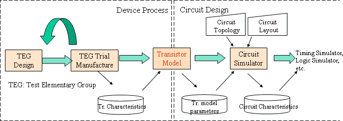
Fig. 1. Role of transistor model
• What a transistor model is
A transistor model is a model to be used for predicting the circuit characteristics in the circuit simulation, describing the electrical properties of a transistor (Fig. 2) with approximate expressions. For instance, the relations of drain current-vs-drain voltage and drain current-vs-gate voltage are described by mathematical expressions. An integrated circuit (IC) consists of a number of transistors combined. When designing an IC, constituent libraries and analog circuits are constructed by using transistor models. See Fig. 1, Circuit Design. The transistor model serves as an interface between circuit design and device manufacture. A transistor model includes a number of model parameters, each of which defines physical size, fundamental characteristic values, coefficients for various physical events, and so on. Numerical data for model parameters are provided by the device maker and the circuit is designed by using these parameters.
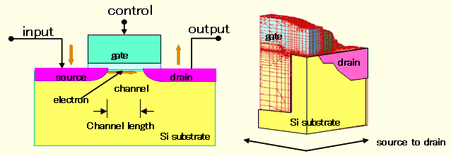
Fig. 2. Construction diagram of a MOSFET
• Problems in conventional transistor model
As the process is refined to a very fine configuration level, it has often been pointed out that the simulation accuracy of the conventional transistor model is not adequate for the ultra-fine transistors and those of very complicated construction. In the current standard model, BISM3, where modeling is made on the basis of drift approximation, effects of physical events having been hitherto ignored become not negligible, making the approximation invalid. Consequently, the model expression grows inevitably more and more complicated for describing various phenomena occurring within a transistor, and BSIM4, a successor version of BSIM3, involves model parameters as many as 400.
While these model parameters are to be provided from device makers to circuit designers, few of them are directly determined through the physical measurement of TEG, and most of model parameters are to be indirectly estimated on the basis of measured electrical properties of transistor. The estimation work is termed “fitting” or “parameter extraction”. See the following paragraph “Image of Fitting Work for Transistor Model”. With the conventional model, even a skilled person takes a week or longer for fitting as many as 400 model parameters. The fitting work is needed every time manufacturing process is changed, transistor construction is modified, or preparatory conditions are altered. This augments the number of steps required for fitting, and takes much more labor for ensuring timely and accurate simulation. The situation is linked to a rise of development cost and provides serious problems. In order to eliminate these obstacles, it is necessary to divide a large number of model parameters into a few groups, to fit parameters in each group separately, and finally, to combine grouped parameters together to achieve overall fitting. However, there is no theoretical method available for grouping parameters, and it is inevitable to resort to the know-how or artisan skill of an experienced designer.
◊ Image of Fitting Work for a Transistor Model
An image of the fitting work is illustrated in Fig. A, where the velocity of an aircraft in the course of acceleration is modeled. The velocity of a flying aircraft is measured at fixed intervals and plotted against time. Based on the plotting, the aircraft is modeled to be flying at a constant acceleration. The velocity-time relationship for this model is represented by a linear expression, with two constants, initial velocity, V0, and acceleration a. These constants are model parameters. The model parameters are to be adjusted so that plotted points of measured velocity fit exactly on the model line. The adjustments constitute fitting or tuning. Once fitting is achieved, it becomes possible to predict velocity (V = Vf) at time (t = tf). The analogy between this example and transistor model fitting may be summarized as following: aircraft velocity vs. electrical properties of transistor, velocity measurement vs. TEG measurement, model expression vs. BSIM or HiSIM, two constants vs. multiple model parameters, and velocity prediction vs. circuit simulation.
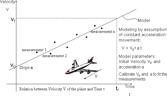
Fig. A. Image of model fitting work, as illustrated by modeling for aircraft velocity.
• Next Generation Transistor Model HiSIM
For resolving these problems, Hiroshima University and STARC have embarked on the joint development of HiSIM as the new generation transistor model. With the HiSIM, it has been attempted to model MOSFET on the basis of surface potential, analyzing the physical principles of transistor as faithfully as possible. As a result, the model description is simplified as a whole, and the number of model parameters is reduced to 70 or so. Moreover, the HiSIM is characterized by flexible coverage for modeling of transistors of more complicated construction, and easier simulation of properties in the high frequency region. In the fitting process for the HiSIM, however, it is necessary in principle to fit in all the model parameters collectively, and the know-how obtained with the previous model fitting is not applicable. Model parameters for the HiSIM are divided into two groups: parameters needed for defining the surface potential, and those required for deciding physical quantities. Since these two groups are mutually dependent for affecting the electrical properties, it is not appropriate to combine two fitting figures having been acquired independently. In order that the HiSIM would work effectively as a new generation transistor model, the automation and the accuracy upgrading constitute key factors.
The ASRC-AIST has been engaged in basic research on fitting technology based on the genetic algorithm since fiscal 2001. On the basis of results obtained through this study, the ASRC-AIST has started from fiscal 2002 R&D works on the automatic fitting technology for ion implantation models in collaboration with Semiconductor Leading Edge Technologies, Inc. (Selete) under the Semiconductor MIRAI Project, and succeeded in automatically fitting 144 model parameters within a few minutes. The results have been commercialized by the ERI in the form of software, which has been incorporated in the three-dimensional TCAD system “ENEXSS” of Selete.
On the other hand, R&D of the HiSIM was initiated in fiscal 1998 by Hiroshima University and STARC and the model was named officially as Hiroshima University STARC IGFET Model (HiSIM) in fiscal 2000. In January 2002, the HiSIM was released to the public on the Web. A new project for developing a new version of HiSIM for high frequency devices has been started in January 2002.
In fiscal 2004, a joint study on the high accuracy automatic fitting for the HiSIM has been commenced by the ASRC-AIST and the Hiroshima University as a part of the Semiconductor MIRAI Project, and the validity of new technology is being verified with measured data of transistors manufactured through the leading edge process provided by STARC.
The automatic fitting technology for the HiSIM jointly developed by the ASRC-AIST and the Hiroshima University is characterized by automatic fitting of multiple parameters in block through the application of genetic algorithm in artificial intelligence, without grouping and combining by human labor. See Fig. 3. The genetic algorithm makes it possible to optimize multiple parameters efficiently preventing the process of searching optimal solution from being trapped by local optimum.
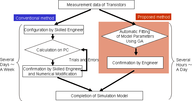
Fig. 3. Comparison of proposed technology with conventional one
In the genetic algorithm, multiple model parameters for the HiSIM are combined together and represented by “01” bit strings, which are regarded as a “chromosome”. See Fig. 4, (Step 1). Multiple chromosomes are provided in a random manner, and the actual transistor characteristics are simulated through the HiSIM by using model parameters in the chromosome concerned. On comparing the simulation characteristics with the measured values the chromosome with smaller error is assigned with greater “fitness value”. See Fig. 4, (Step 2). Then, chromosomes with greater fitness values are “mated” to cause “crossover” or “mutation”. Fitness values of newly created chromosomes are computed, the chromosome with lowest fitness value is eliminated, and a new chromosome is added to the search candidates. See Fig. 4, (Step 3). A series of steps including fitness evaluation, cross-over and selection is termed “generation”. As the generation is repeated, chromosomes of higher fitness, that is, a group of model parameters with smaller errors from the measured values are obtained in block.
In the actual experiment, it has been attempted to fit 32 major model parameters* for the HiSIM to the current characteristics of the transistor. The current characteristics data have been provided by STARC as measured for transistors manufactured in accordance with the 90 nm rule: (eight transistors of different dimensions: channel length 100 nm ~ 10 _m and channel width 2 _m) (1_m = 1/1,000,000 m). With an ideal model, the error between the measured value and the HiSTM simulation is to be zero, and parameter values are to be adjusted so as to minimize the error. The experiment proved that the parameters were closely fitted for the drain current-drain voltage characteristics of transistors with 100 nm channel length (Fig. 5) and for the drain current-gate voltage characteristics of transistors with 100 nm channel length (Fig. 6). For all the transistor sizes including channel length 100 nm, the current characteristics showed agreement between simulated and measured values within 2.5 % of RMS error (Table. 1). In this way, accurate circuit simulation will be available for designing complicated system LSI including MOSFET of different transistor sizes. The fitting work took 23 hours or so with a single PC, and within 3 hours when using a cluster involving eight PCs. It is evident, therefore, that the fitting work having required a few days to a week or so even with a skilled designer may be shortened and automated.