Update(MM/DD/YYYY):01/17/2006
Successful Development of an Upright-type Double-gate MOS Transistor Capable of Ultra-large scale integration
- 30% upgrade in performance using the soft neutral beam technique, paving the way for the 32-nanometer technology generation -
Key Points
-
We have established a high-precision fine-etching technique using soft neutral beams which cannot damage silicon substrates.
-
Using this technique, we have successfully manufactured an upright-type double-gate MOS transistor capable of ultra-large scale integration, and its performance is 30% better than that of transistors produced with conventional manufacturing techniques.
-
This technique will pave the way for the 32-nanometer technology generation.
Synopsis
The National Institute for Advanced Industrial Science and Technology (AIST, President: Hiroyuki Yoshikawa) and Tohoku University (President: Takashi Yoshimoto) have succeeded in manufacturing a high-performance upright-type double gate MOS transistor capable of ultra-large scale integration using neutral beams which cannot damage silicon substrates.
In the semiconductor industry, global competition for developing and miniaturizing new materials has been increasing. Silicone plays a particularly important role for driving the semiconductor industry, so research and development of high performance silicone are very important for outpacing the competition. Successful development requires the miniaturization of high-performance integrated circuits. However, with conventional techniques designed for the fabrication of 2D-spreading devices, the amount of heat caused by leakage-current from the miniaturized circuit elements is so great that it is extremely difficult to develop ultra-large scale integration circuits for the 32-nm technology generation.
To overcome such a technical barrier, AIST has been developing a 3D, upright-type double-gate MOS transistor, which not only can suppress the leakage-current that causes heat generation but can be highly integrated. Thus, combining this AIST technique with a nearly damage-free etching technique using neutral beams, which has been developed by Prof. Seiji Samukawa of Tohoku University, we have created an upright-type double-gate MOS transistor which enables ultra-large scale integration.
This transistor has an etched surface flatness of less than 1 nm in irregularity, and has high electron mobility. Moreover, the performance of the transistor was found to be 30% better than that of the transistors fabricated by conventional processing techniques. This suggests that our technique may be promising for ultra-fine circuit fabrication in the 32-nm technology generation.
 |
 |
|
An upright-type double-gate MOS transistor fabricated experimentally.
|
This work was presented on December 7 at the 2005 International Electron Device Meeting, which was held at Washington, DC from December 5 to 7.
Background of Research Work
When conventional planar-type bulk MOS transistors are used for the 32 nm-node integrated circuits expected to be in practical use from 2013, it is very difficult to provide the complete shielding of the leakage current at the operation-off time, indicating that there is a limit for ultra-large scale integration. Thus, promising 3D structural devices like double-gate MOS transistors with upright channels have been developed globally.
AIST first proposed a double gate transistor called "XMOS" in 1984, which is suitable for ultra-large scale integration. After verifying its principle, we developed a 3D, upright-type, double-gate transistor which can be produced relatively easily. However, when conventional plasma etching is used, the 3D upright channels are vulnerable to damage, deformation, and surface roughness during their manufacture, posing serious obstacles for the ultra-fine miniaturization of the devices. These obstacles must be overcome to achieve ultra-micro fabrication.
History of Research Work
AIST created a prototype double-gate transistor called XMOS in the days of the former ETL in 1984, and has since developed it into an upright-type, double-gate transistor. With this transistor, multiple gates can be accurately opposed easily; thus it has been attracting much attention worldwide as an ultimate transistor with ultra-fine structures which can overcome the limitations on miniaturization. However, when conventional plasma etching techniques are used, fabricated surfaces become rough, making the ultra-micro fabrication difficult. Thus, a way of overcoming that has been sought.
Early on, Prof. Seiji Samukawa of Tohoku University noticed disadvantages of plasma etching techniques, such as plasma damage and product deformation. Thus, he began studying etching techniques using neutral beams obtained by electrical neutralization of plasma. As a result, he has established a practical technique for the effective generation of neutral beams using negative ions. Furthermore, he has succeeded in the development of an etching technique utilizing soft neutral beams which cannot damage silicon substrates.
Combining these techniques, AIST and Tohoku University have attempted to apply the neutral beam technique to the fabrication of an upright-type (so-called "Fin-type") double gate MOS transistor.
Details of Research Work
An overview of the upright-type double-gate MOS transistor we have developed is shown in Figure 1. This transistor has a 3D (Fin) structure in which the channels stand vertically to the silicon substrate. High-performance transistors with such an ultra-fine structure cannot be fabricated with conventional plasma etching, because the fine structure can be damaged by high-energy plasma and ultraviolet light radiating from the plasma.
To resolve this problem, AIST and Tohoku University applied a soft (or low kinetic energy) neutral beam technique to the fabrication of an upright-type double-gate MOS transistor, leading to first successful production of this transistor in the world.
Figure 2 shows an overview of the neutral beam generation equipment we used. With this equipment, negatively charged chloride ions can be generated effectively from time-modulated chloride plasma, and then accelerated and effectively neutralized on the lower electrode made of a carbon plate to be radiated to substrates. Also, the kinetic energy of the particles can be controlled by varying bias voltage, enabling almost damage-free etching of silicone substrates that has lead to the successful fabrication of the Fin part that has an ultra-fine 3D structure
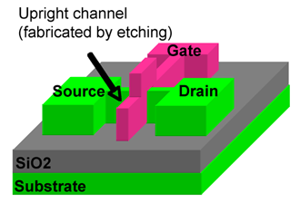
Figure 1 Schematic diagram of the upright double-gate MOS transistor ("Fin type")
|
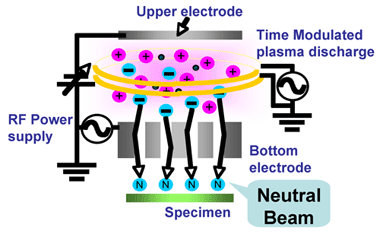
Figure 2 Equipment for neutral beam generation
|
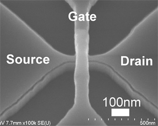
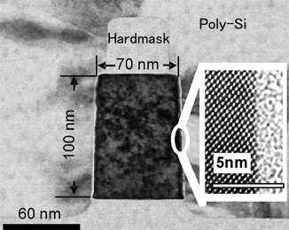
Figure 3 shows an SEM image of the upright-type double-gate MOS transistor we have developed. Figure 4 shows a TEM image of the channel part of the transistor. As seen from the magnified inset in this figure, the channel through which electrons pass is flat in atomic level (the black circles correspond to silicone atoms, demonstrating that the silicone substrate is fabricated almost completely without damage.
Figure 3 An SEM image of the upright-type double-gate MOS transistor we have developed
|
Figure 4 A TEM image of the channel cross-section
|
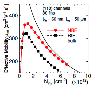
Figure 5 shows the mobility of electrons in the channel of the experimental transistor. Electron mobility is a significant index indicating the performance of transistors; when this value is large, the transistors can be operated with low voltages without reducing the performance, leading to the suppression of heat generated from device elements. Thus, the mobility of electrons in the channel is an important index.
The electron mobility of the transistor we have developed is 30% greater than that of conventional transistors (corresponding to the difference between the peak values of the black and red curves), and is close to the ideal electron mobility. This suggests that the barrier for 32 nm node device fabrication has been overcome, and thus indicates that a solution may be found for the ultra-large scale integration of the devices.
 |
|
Figure 5 Comparison of the electron mobility, as a function of inversion charge, of a transistor fabricated using a neutral beam etching method with the mobility of a transistor fabricated with the conventional plasma etching method. The peak value for our transistor is 30% larger than that of the conventional transistor, and is much closer to the ideal value.
|
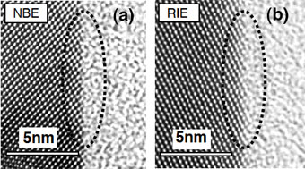
Figure 6 A TEM image for a sidewall cross-section of silicon after etching
|
The increase in the electron mobility may be caused by atomic-scale flattening of the channel surface with neutral beam etching. We think that the electrons can move without scattering therein due to the atomic-scale flatness, resulting in a dramatic* increase in the electron mobility.