Kazutomo Suenaga (Prime Senior Researcher) of the Nanotube Research Center (NTRC; Director: Sumio Iijima) of the National Institute of Advanced Industrial Science and Technology (AIST; President: Ryoji Chubachi) and Ryosuke Senga (Researcher) of the Nano-carbon Characterization Team, NTRC, AIST, have synthesized an atomic chain in which two elements are aligned alternately and have evaluated its physical properties on an atomic level.
An ionic crystalline atomic chain of cesium iodine (CsI) has been synthesized by aligning a cesium ion (Cs+), a cation and an iodine ion (I-), an anion, alternately by encapsulating CsI in the microscopic space inside a carbon nanotube. Furthermore, by using an advanced aberration-corrected electron microscope, the physical phenomena unique to the CsI atomic chain, such as the difference in dynamic behavior of its cations and anions, have been discovered. In addition, from theoretical calculation using density functional theory (DFT), this CsI atomic chain has been found to indicate different optical properties from a three-dimensional CsI crystal, and applications to new optical devices are anticipated.
This research has been conducted as a part of both the Strategic Basic Research Program of the Japan Science and Technology Agency and the Grants-in-aid for Scientific Research of the Japan Society for the Promotion of Science. The details of the study was published online in Nature Materials on September 15, 2014 (Japan Standard Time).
 |
|
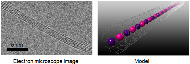
Actual electron microscope image and model of CsI atomic chain encapsulated inside carbon nanotube |
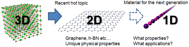
In the accelerating and ballooning information society, electronic devices used in computers and smartphones has constantly demanded higher performance and efficiency. The materials currently drawing expectations are low-dimensional materials with a single to few-atom width and thickness. Two-dimensional materials, typified by graphene, indicate unique physical characteristics not found in three-dimensional materials, such as its excellent electrical transport properties, and are being extensively researched.
An atomic chain, which has an even finer structure with a width of only one atom, has been predicted to display excellent electrical transport properties, like two-dimensional materials. Although expectations were higher than for two-dimensional materials from the viewpoint of integration, it had attracted little attention until now. This is because of the technological difficulties faced by the various processes of academic research from synthesis to analysis of atomic chains, and academic understanding has not progressed far (Fig. 1).
 |
|
Figure 1 : Transition of target materials in material research |
AIST has been developing element analysis methods on a single-atom level to detect certain special structures including impurities, dopants and defects, that affect the properties of low-dimensional materials such as carbon nanotubes and graphene (AIST press releases on July 6, 2009, January 12, 2010, December 16, 2010 and July 9, 2012). In this research, efforts were made for the synthesis and analysis of the atomic chain, a low-dimensional material, using the accumulated technological expertise. This research has been supported by both the Strategic Basic Research Program of the Japan Science and Technology Agency (FY2012 to FY2016), and the Grants-in-aid for Scientific Research of the Japan Society for the Promotion of Science, “Development of elemental technology for the atomic-scale evaluation and application of low-dimensional materials using nano-space” (FY2014 to FY2016).
The developed technology is the technology to expose carbon nanotubes, with a diameter of 1 nm or smaller, to CsI vapor to encapsulate CsI in the microscopic space inside the carbon nanotubes, to synthesize an atomic chain in which two elements, Cs and I, are aligned alternately. Furthermore, by combining aberration-corrected electron microscopy and an electronic spectroscopic technique known as electron energy-loss spectroscopy (EELS) detailed structural analysis of this atomic chain was conducted. In order to identify each atom aligned at a distance of 1 nm or less without destroying them, the accelerating voltage of the electron microscope was significantly lowered to 60 kV to reduce damage to the sample by electron beams, while maintaining sufficient spatial resolution of around 1 nm. Figure 2 indicates the smallest CsI crystal confirmed so far, and the CsI atomic chain synthesized in this research.
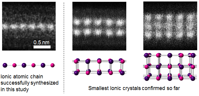 |
Figure 2 : Comparison of CsI atomic chain and CsI crystal
(Top: Actual annular dark-field images, Bottom: Corresponding models) |
Figure 3 shows the annular dark-field (ADF) image of the CsI atomic chain and the element mapping for Cs and I, respectively, obtained by EELS. It can be seen that the two elements are aligned alternately. There has not been any report of this simple and ideal structure actually being produced and observed, and it can be said to be a fundamental, important finding in material science.
Normally, in an ADF image, those with larger atomic numbers appear brighter. However, in this CsI atomic chain, I (atomic number 53) appears brighter than Cs (atomic number 55). This is because Cs, being a cation, moves more actively (more accurately, the total amount of electrons scattered by the Cs atom is not very different from those of the I atom, but the electrons scattered by the moving Cs atom generate spatial expansion), indicating a difference in dynamic behavior of the cation and the anion that cannot occur in a large three-dimensional crystal. Locations where single Cs atom or I atom is absent, namely vacancies, were also found (Fig. 3, right).
The unique behavior and structure influence various physical properties. When optical absorption spectra were calculated using DFT, the response of the CsI atomic chain to light differed with the direction of incidence. Furthermore, it was found that in a CsI atomic chain with vacancies, the electron state of vacancy sites where the I atom is absent possess a donor level at which electrons were easily released, while vacancy sites where the Cs atom is absent possess a receptor level at which electrons were easily received. By making use of these physical properties, applications to new electro-optical devices, such as a micro-light source and an optical switch using light emission from a single vacancy in the CsI atomic chain, are conceivable. In addition, further research into combinations of other elements triggered by the present results may lead to the development of new materials and device applications. There are expectations for atomic chains to be the next-generation materials for devices in search of further miniaturization and integration.
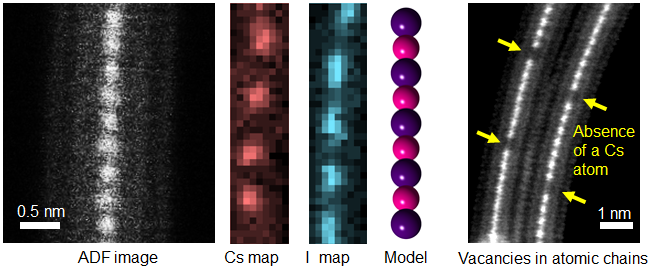 |
Figure 3 : Synthesized CsI atomic chain, encapsulated in double-walled carbon nanotube
(From left: ADF image, element maps for Cs and I, model, ADF image of CsI atomic chains with vacancies) |
Since the CsI atomic chain displays optical properties significantly different from large crystals that can be seen by the human eye, there are expectations for its application for new electro-optical devices such as a micro-light source and an optical switch using light emission from a single vacancy in the CsI atomic chain. The researchers will conduct experimental research in its application, focused on detailed study of its various physical properties, starting with its optical properties. In addition to CsI, efforts will also be made in the development of new materials that combine various elements, by applying this technology to other materials.
Furthermore, the mechanism of all adsorbents of radioactive substances (carbon nanotubes, zeolite, Prussian blue, etc.) currently being developed for commercial use are methods of encapsulating radioactive atoms inside microscopic space in the material. The researchers hope to utilize the knowledge of the behavior of the Cs atom in a microscopic space obtained in this research, to improve adsorption performance.