Update(MM/DD/YYYY):09/03/2014
Development of a Method for High-accuracy Measurement of Impurity Concentration Distribution of Microscopic Transistors
- Contributes to development of next-generation semiconductor transistors -
Points
-
Simulation of semiconductor transistor measurement using a scanning tunneling microscope
-
Compensates for the effect of current flowing through the sample when measuring, by simulation
-
Contributes to the development of next-generation transistor through high-accuracy measurement of impurity distribution in a nanometer order
Summary
Tetsuya Tada (Leader) and Koichi Fukuda (Senior Researcher), the Nanoscale Characterization and Processing Research Group, the Nanoelectronics Research Institute (Director: Tetsuji Yasuda) of the National Institute of Advanced Industrial Science and Technology (AIST; President: Ryoji Chubachi), have developed a scanning tunneling microscope (STM) simulation technology for high-accuracy measurement of impurity concentration distribution in microscopic transistors.
Because STM can measure tunneling current that reflects the electrostatic potential of the semiconductor sample surface and the carrier concentration within the semiconductor, utilization is expected in the measurement of dopant impurity concentration distribution in microscopic transistors. However, STM requires voltage to be applied to the sample for measurement, making accurate measurement of potential distribution impossible because the applied voltage and the current that runs through the sample change the potential distribution of the sample. Therefore, to obtain the correct potential distribution, there was a need to remove these effects. The developed simulation technology enables the removal of the effects of the voltage applied between the STM probe and the semiconductor sample using computer simulation, in particular, the effects of the tunneling current that flows between the probe and the sample also flowing inside the sample. Using the technology has enabled high-accuracy measurement of potential and impurity concentration distribution using STM. As this will allow accurate measurement in a nanometer order, contribution to the development of next-generation transistors is expected.
Details of this technology will be published in a scientific journal of the American Institute of Physics, Journal of Applied Physics, in the near future.
 |
Computer simulation of STM measurement of a semiconductor sample
Current in accordance with impurity concentration of the probe location is obtained from calculation that includes the probe and the semiconductor sample. |
Social Background of Research
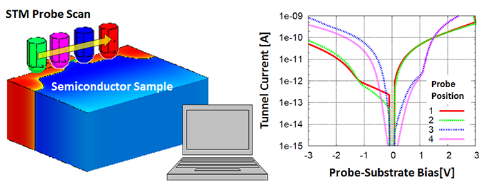
With the recent developments in large-scale integrated circuits (LSIs), the miniaturization of transistors is now approaching its limit, requiring high-precision control of impurity dopants. This requires the measurement of impurity concentration distribution at a high spatial resolution and STM has been attracting attention as a non-destructive method for high-spatial-resolution measurement. A conceptual drawing of STM measurement is shown in Fig. 1. When voltage is applied between the semiconductor sample and the STM probe, tunneling current will flow, dependent on the electrostatic potential of the sample surface and the carrier concentration immediately below the probe. It was expected that because STM uses a probe for scanning, the tunneling current, reflecting the impurity concentration of each location, would allow the n-type and p-type impurity concentration distribution to be measured.
However, because voltage is applied between the STM probe and the sample, with the effects of applied voltage and tunneling current running through the sample, the electrostatic potential and carrier concentration immediately below the probe will change, and the actual impurity concentration cannot be obtained. Computer simulation was required to remove such effects, but until now, although proposals had been made to solve this on an atomic scale through STM simulation, there was no computer simulation technology that allowed the analysis of effects of current flowing widely within the semiconductor sample.
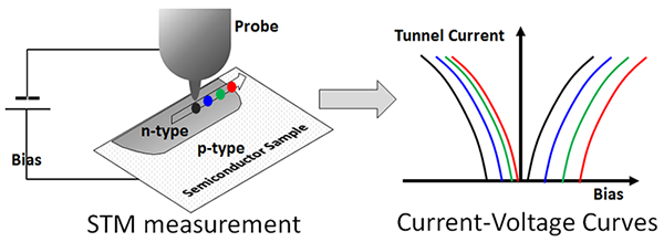 |
Figure 1 : Conceptual drawing of STM measurement of a semiconductor sample
Tunneling current reflects the impurity concentration, such as n-type or p-type, immediately below
the probe. The current-voltage curves for each location indicated in the figure on the left will differ
in accordance with the impurity concentration of the location, as indicated in the figure on the right. |
History of Research
The Nanoscale Characterization and Processing Research Group of the Nanoelectronics Research Institute of AIST has been developing methods to measure physical quantities at a nanometer order of accuracy by applying TCAD technology, a computer simulation technology, to high-accuracy physical analysis of microscopic semiconductor devices.
In this research, development of a computer simulation technology to reproduce and analyze STM measurement as accurately as possible was conducted using a research method to narrow down critical factors, by postulating the cause of the difference with the measured values.
Details of Research
The developed STM simulator sets the structure of the semiconductor sample and the STM probe by semiconductor production process simulation. By the input of STM measurement conditions, STM measurement procedures, such as the automatic adjustment of the distance between the sample and the probe or the scanning of the probe, are automatically reproduced to predict the tunneling current-voltage curves by semiconductor device simulation.
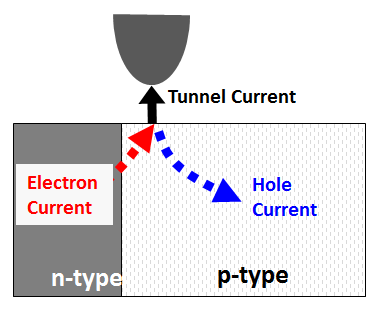
Figure 2 shows a conceptual drawing of current calculation in the simulation. Incorporating the semiconductor device simulation has enabled the calculation of tunneling current flowing between the sample and the probe, and the electron and hole currents flowing in the semiconductor without inconsistencies.
 |
|
Figure 2 : Conceptual drawing of current calculation of the simulation |
Figure 3 shows the current-voltage curve measured by STM for a semiconductor sample of known impurity concentration (indicated with ● markers) and the predicted values obtained from the developed simulation (indicated with a solid line). It has been demonstrated that considering the effects of the current within the semiconductor makes it possible to calculate the measured values for the semiconductor sample accurately for the first time.
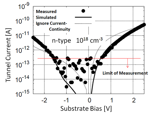 |
Figure 3 : Current-voltage curve (points) of a semiconductor sample measured by STM and the simulation results (solid line)
Simulation reproduces the measurement results with good accuracy. (measuring limit reached at 3 x 10-13[A]).
The dotted line indicates simulation results disregarding the spread of current, and does not match measured values. |
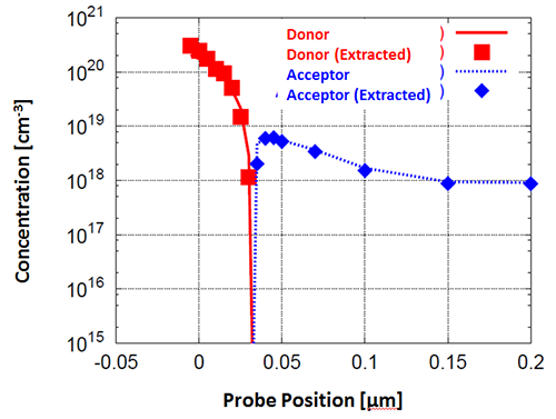
Figure 4 indicates the results of a computer simulation test to estimate impurity distribution using the developed technology. Impurity concentration distribution of the n-p junction is assumed by the semiconductor manufacturing process simulation (indicated by lines) and then STM measurement results were predicted using the developed simulator. From the predicted STM measurement results, the concentration distribution was obtained in reverse, using the developed simulation technology, and compared with the concentration distribution assumed at the beginning. Starting from an initial value of impurity distribution different from the assumed impurity distribution, the obtained concentration distribution is indicated by markers. The obtained concentration distribution matches the initial assumed concentration very well with accuracy in the order of 0.01 μm (10 nm). As indicated, the impurity distribution of a semiconductor sample can be estimated with high accuracy with STM measurement by using the developed simulator.
 |
|
Figure 4 : Results of estimation test of an n-p junction impurity distribution |
Future Plans
The developed STM simulation technology will be provided to developers of semiconductor devices to accelerate the achievement of microscopic devices, as well as being provided to STM measurers, to contribute to improvements in measuring methods. In addition, it will be used as a common infrastructure for research into further development of next-generation technologies, in collaboration with the industrial and academic sectors, at Tsukuba Innovation Arena for Nanotechnology (TIA-nano) and AIST Super Clean Room Collaboration Building.